Table of Contents for
Electronics Cookbook
 Electronics Cookbook
Published by
O'Reilly Media, Inc., 2017
Electronics Cookbook
Published by
O'Reilly Media, Inc., 2017
- Cover
- nav
- Electronics Cookbook
- Electronics Cookbook
- Preface
- Theory
- Resistors
- Capacitors and Inductors
- Diodes
- Transistors and Integrated Circuits
- Switches and Relays
- Power Supplies
- Batteries
- Solar Power
- Arduino and Raspberry Pi
- Switching
- Sensors
- Motors
- LEDs and Displays
- Digital ICs
- Analog
- Operational Amplifiers
- Audio
- Radio Frequency
- Construction
- Tools
- Parts and Suppliers
- Arduino Pinouts
- Raspberry Pi Pinouts
- Units and Prefixes
- Index
- About the Author
- Colophon
Chapter 20. Construction
20.1 Create Temporary Circuits
Solution
Using a solderless breadboard (Figure 20-1) is a great way to temporarily build an electronic design because you can easily swap out different components without having to desolder (Recipe 20.6). Once the design is right it can be transferred either to a prototyping board (Recipe 20.2) or a circuit board of your own design (Recipe 20.3).
Breadboards are available in many shapes and sizes. I recommend having a good supply of 400-point breadboards (often called half-breadboards) as these are a great size to accommodate a couple of chips and a whole load of components. For those situations where you need more prototyping area breadboards can be clipped together.
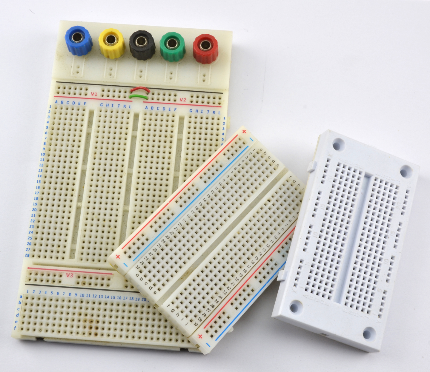
Figure 20-1. A Selection of Breadboards
Figure 20-2 shows how a 400-point breadboard is constructed of rows of five holes, all connected together by a clip. Note that there is a break in connectivity between “abcde” and “fghij.”
The “supply rails” in pairs down the sides of the board are all connected together and can be used for any purpose, but generally the ones marked in blue or with a “–” next to them are used for ground and the red ones marked with a “+” are used for the positive supply.
The rows and columns of the breadboard are labeled with numbers and letters, making it easier to transfer the designs to a more permanent design using Permaproto or Monk Makes Protoboard. These are general-purpose circuit boards with the same layout as breadboards.
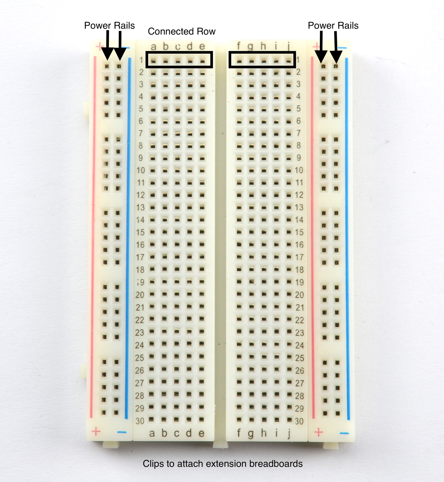
Figure 20-2. The “Half-Breadboard” Layout
Figure 20-3 shows the two-transistor oscillator from Recipe 16.2 built on a breadboard.
Through-hole component leads are pushed into holes on the breadboard and connected to other component leads either by being in the same breadboard row, or by using male-to-male jumper wires to link one part of the board to another.
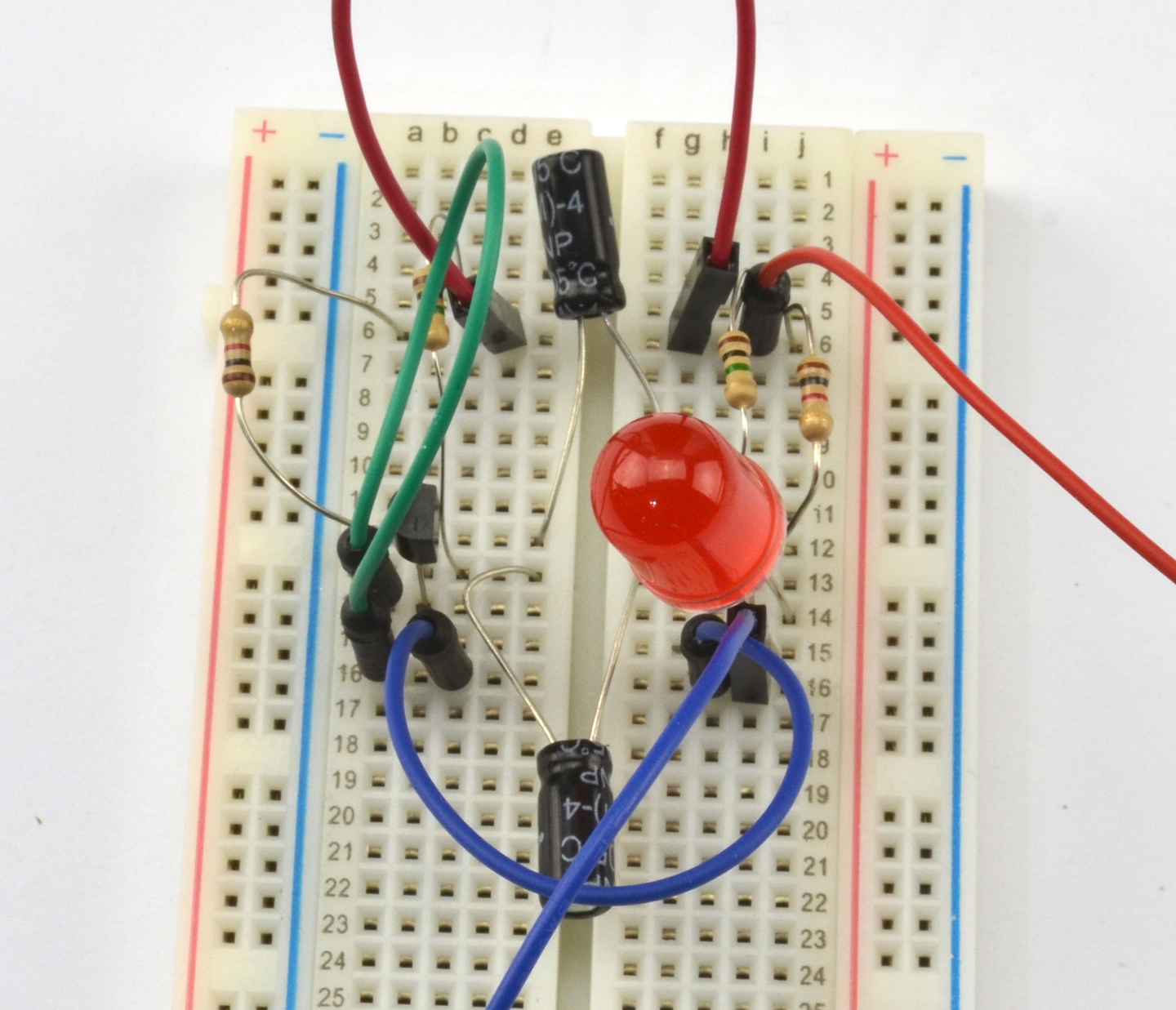
Figure 20-3. Building a Circuit on a Breadboard
There is a bit of craft involved in the mental conversion of a schematic to a breadboard layout. Figure 20-4 shows the schematic layout for Recipe 16.2 and Figure 20-5 the one corresponding to the breadboard layout (also shown in Figure 20-3).
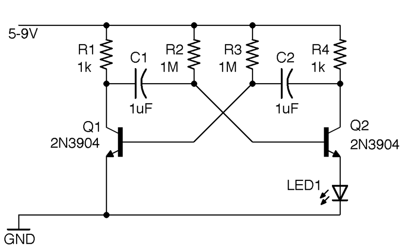
Figure 20-4. Schematic for a Transistor Oscillator
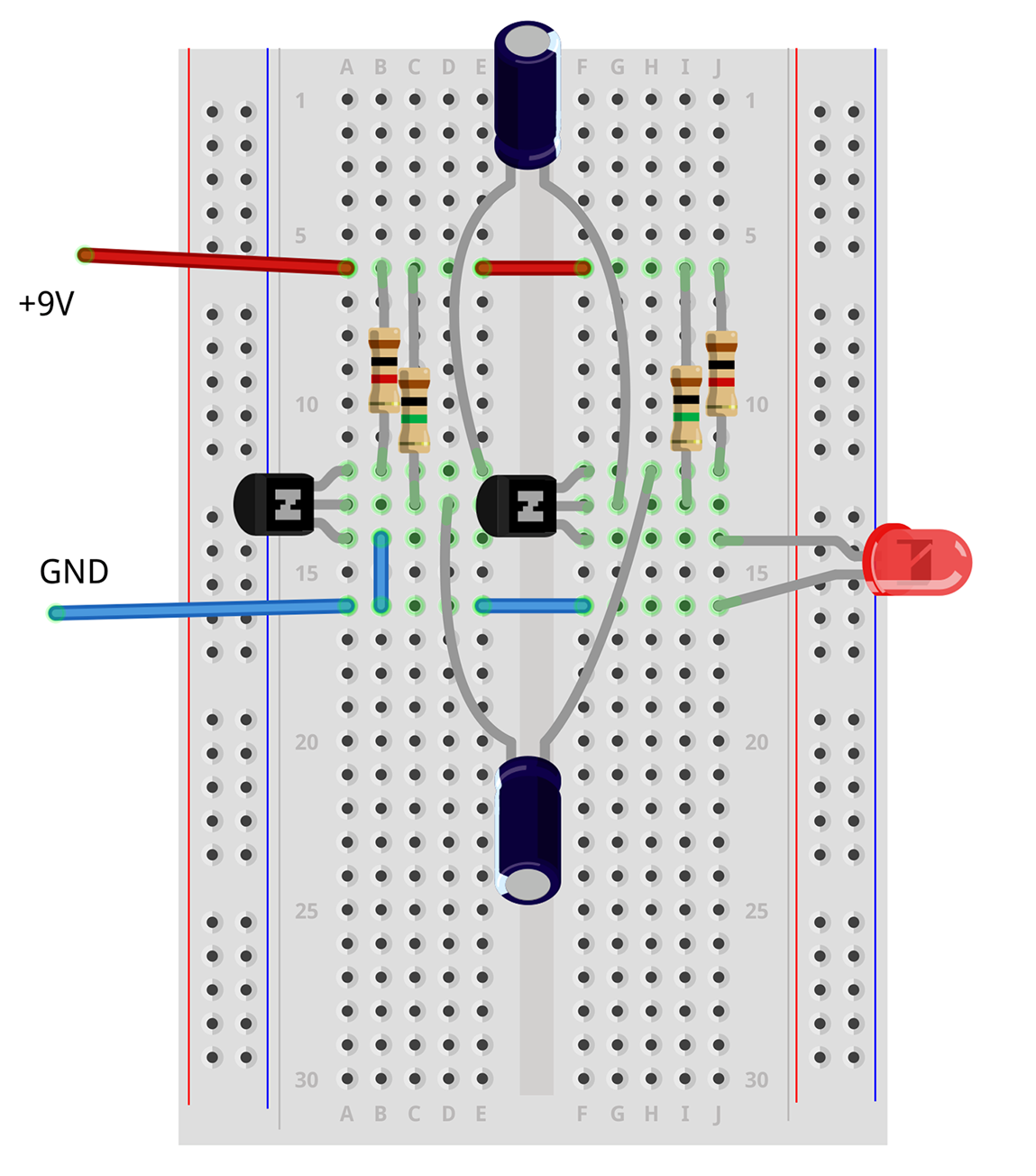
Figure 20-5. Breadboard Layout for a Transistor Oscillator
When transferring a schematic to a breadboard, I start with the key components and the ones whose legs won’t bend very far. Usually this means starting with any ICs, but in this case, it means the transistors, which I have placed on opposite halves of the breadboard, mirroring the schematic.
Then I add the other components and jumper wires. There is no hard and fast method for this layout, and of course, being solderless, it’s very easy to change things around if you run out of room.
Discussion
Figure 20-5 was drawn using an open source software tool called Fritzing. This tool produces great-looking diagrams and also allows you to view the same circuit as a schematic, breadboard, or circuit board design, allowing you to use the same software right through from prototyping to circuit board.
When it comes to connecting a breadboard to an Arduino or Raspberry Pi, you can use male-to-male or male-to-female jumper wires, respectively. Figure 20-6 shows Recipe 12.12 on a breadboard connected to a Raspberry Pi.
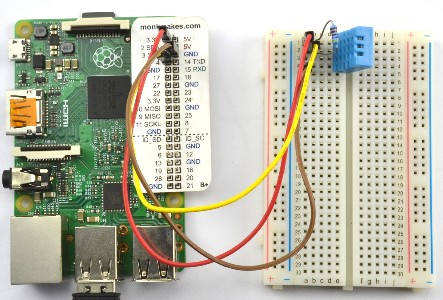
Figure 20-6. Connecting a Breadboard to a Raspberry Pi
Figure 20-7 shows an Arduino Micro on a solderless breadboard. This is one of several models of Arduino including the “mini” and “nano” models that are “breadboard friendly.”
The breadboard shown in Figure 20-3 is likely to have proper electronic engineers holding their heads in their hands and gritting their teeth. The problem with it is that it is all too easy for a component lead to touch another lead that it shouldn’t or simply fall out. This type of arrangement requires care to make sure nothing is touching that shouldn’t be but is fine while you are getting something working. For a halfway house before you move to a soldered prototype, you can take a neater approach and use solid-core wire trimmed to just the right length to lie flat on the breadboard instead of using jumper wires. You can also trim all the component legs so that they are just the right lengths, but this can make them difficult to reuse in your next design.
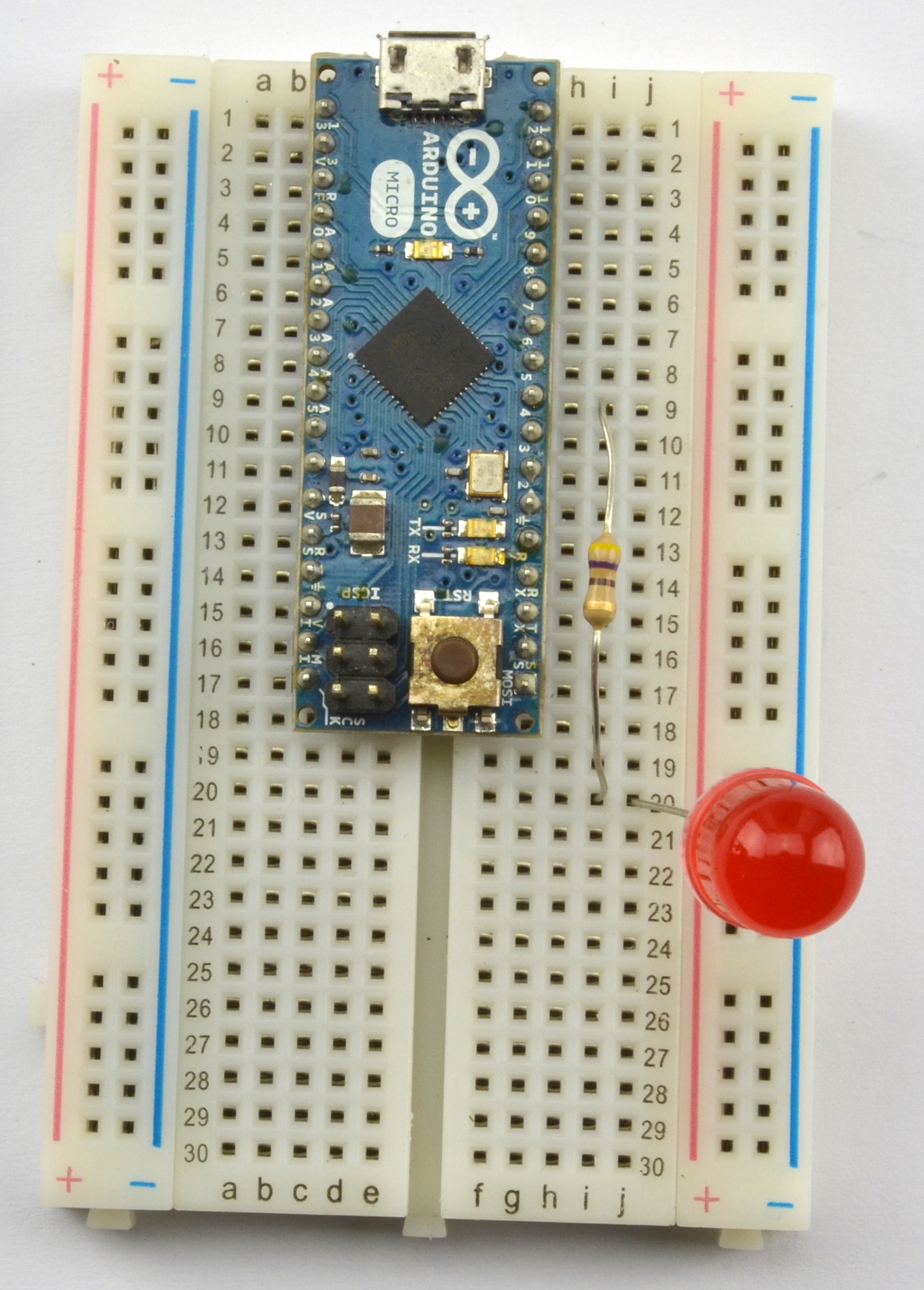
Figure 20-7. An Arduino Micro on a Breadboard
See Also
For more information on Fritzing see http://fritzing.org or my book Fritzing for Inventors, TAB DIY, 2015.
When you are ready to transfer your design to a soldered prototype follow Recipe 20.2.
20.2 Create Permanent Circuits
Solution
Use a prototyping board or protoboard such as the Adafruit Permaproto or the Monk Makes Protoboard and simply transfer the components from their positions on the breadboard to the same locations on the protoboard.
Figure 20-8 shows the starting point for this process of transferring the design from a breadboard to a Monk Makes Protoboard. The details of the design are not important, but for those interested, it is an energy monitor using a particle photon Arduino-like board, a current sensor, and an AC transformer. Note that the breadboard itself is attached to a Monk Makes Protoboard to allow use of the screw terminal and audio-type socket to connect the current sensor and AC transformer to the prototype.
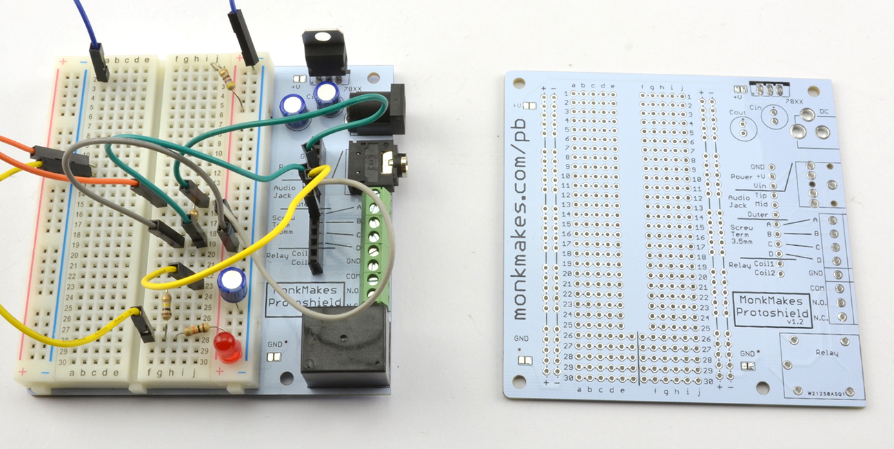
Figure 20-8. The Prototype on a Breadboard
The components can then be moved from the breadboard one at a time, making note of the lead’s row and column coordinates and soldering them onto the Monk Makes Protoboard as shown in Figure 20-9. Finally, Figure 20-10 shows the completed board and the bare breadboard ready for your next project.
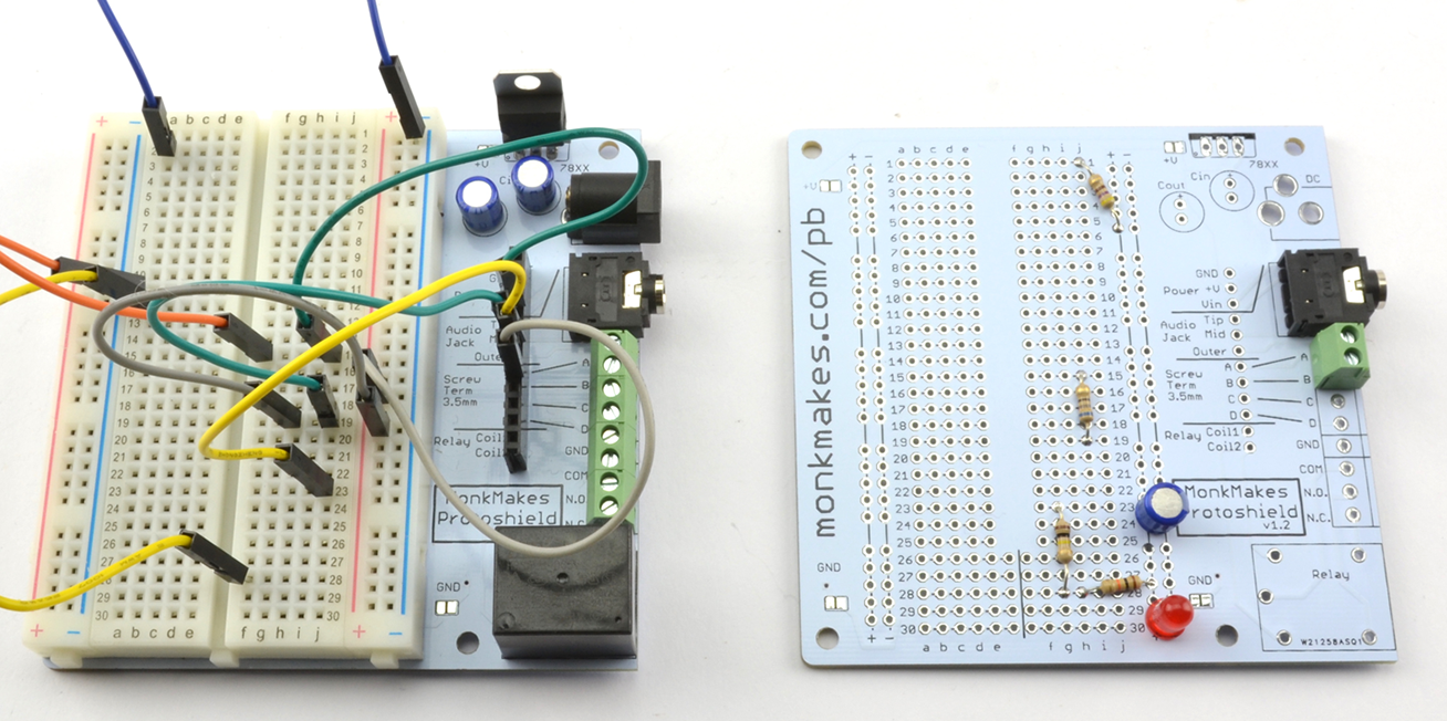
Figure 20-9. Transferring the Components to the Protoboard
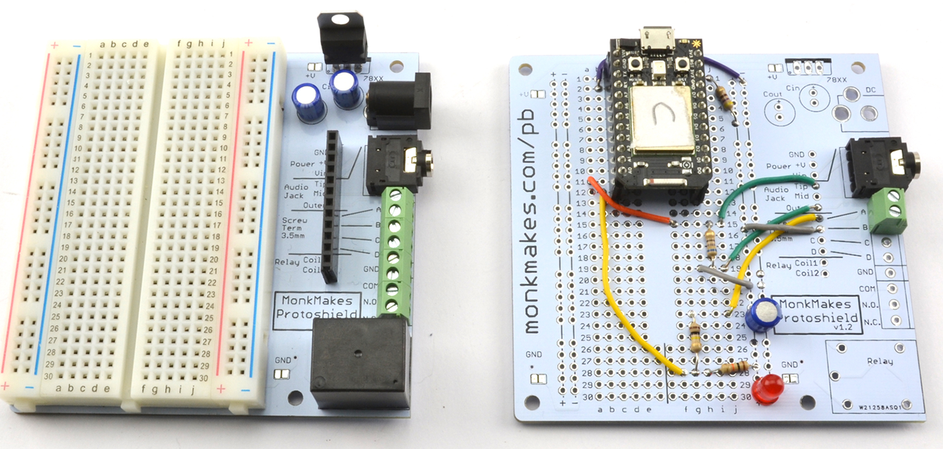
Figure 20-10. The Completed Protoboard
Discussion
Other useful prototyping boards are available including Permaproto boards from Adafruit that are designed to be attached by a ribbon connector to a Raspberry Pi.
When it comes to Arduino, the Arduino Protoshield is a great way to build something and then plug it as a whole board into the top of an Arduino Uno. Figure 20-11 shows a Protoshield with an LED cube project built onto it. The Protoshield is then attached to an Arduino.
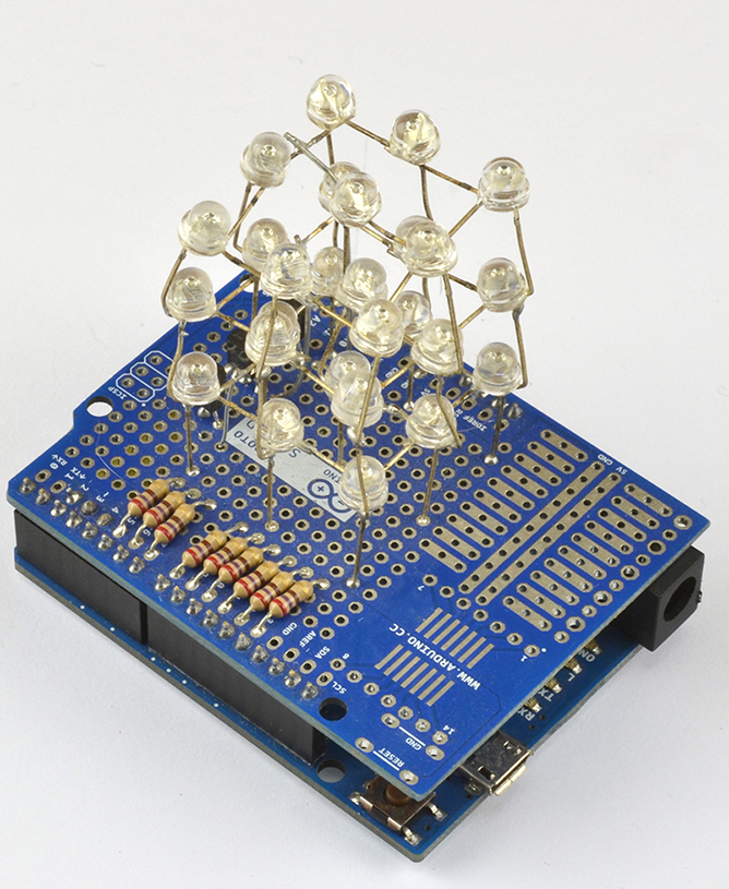
Figure 20-11. An Arduino Protoshield LED Cube
Another popular method for making soldered prototypes is to use stripboard. Stripboard (Figure 20-12 and Figure 20-13) is arranged with copper tracks in rows and can be cut to whatever size you need for your project. Breaks in the track are made using a tool called a “spot cutter” or by using a drill bit rotated by hand just enough to cut the copper.
Figure 20-12. Stripboard (top side)
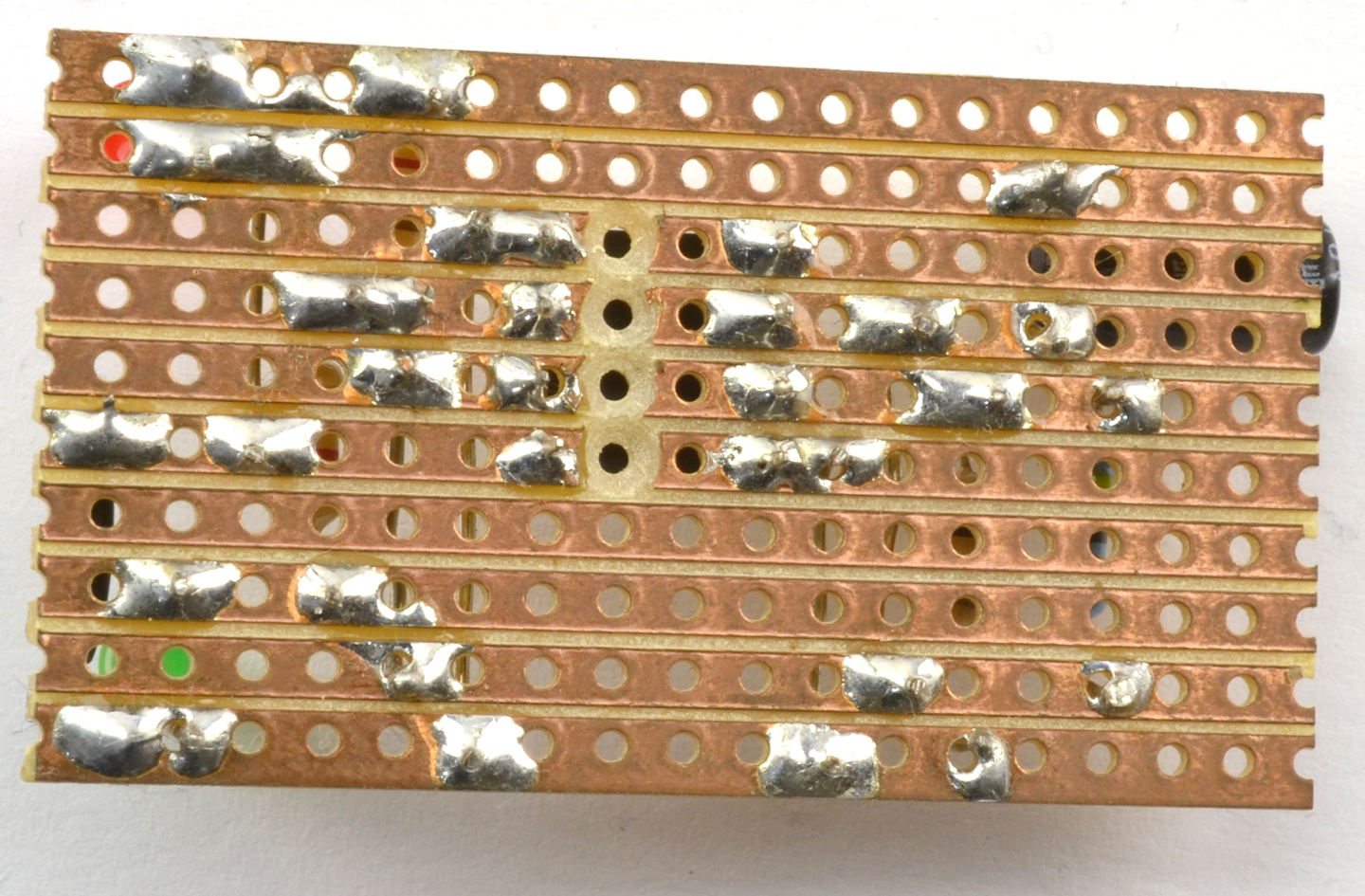
Figure 20-13. Stripboard (under-side)
Perfboard (i.e., perforated board) is like stripboard, but without the copper strips on the back. All connections are made by bending the component leads or lengths of solid-core wire.
Protoboard, which is a variation on perfboard with a separate pad behind each hole, is also available.
See Also
For Permaproto see: https://www.adafruit.com/product/571.
For Monk Makes Protoboard see: https://www.monkmakes.com/pb/
The LED cube project is taken from my book The TAB Book of Arduino Projects, TAB DIY, 2015.
20.3 Design Your Own Circuit Board
Solution
While the solution to this recipe cannot fit into one recipe, you can start by using circuit board design software such as CadSoft EAGLE to draw the schematic for your boards and then layout a circuit board. You can then send away the design files (known as Gerbers) to a circuit board fabrication provider.
Designing a simple circuit board is well within the reach of the amateur. If you restrict yourself to two copper layers, then you can use one of many CAD (computer-aided design) packages for circuit board design.
Perhaps the most popular CAD system is EAGLE CAD (Figure 20-14), which is not open source, but there is a free version for noncommercial projects. One advantage of using EAGLE CAD is that it has been adopted by the open source hardware movement as their CAD system of choice and there are many OSH designs for which the EAGLE design files are available for download, which you can adapt to your own needs. EAGLE is not an intuitive piece of software. If you have used any other circuit board design software, you may be able to find your way around unaided, but typically you will need to follow a few tutorials step-by-step before it really starts to make sense.
Nearly all the schematic diagrams in this book were drawn with EAGLE and once you are familiar with all its quirks, you will probably grow to enjoy using it.
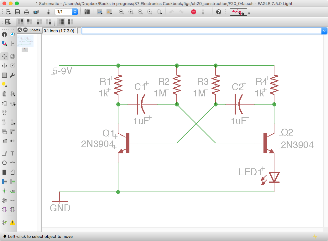
Figure 20-14. The EAGLE CAD Schematic Design Editor
For open source enthusiasts KiCad is a fully featured open source equivalent to EAGLE, and it can import some EAGLE file formats. Like EAGLE, don’t expect to have a finished board design ten minutes after downloading the software.
DesignSpark is a free-ish CAD system that is gaining in popularity and is relatively easy to use, but it does inflict adverts on users.
If you have a really simple circuit board design to make that uses fairly common components, then Fritzing will take you to circuit board design via schematic and breadboard and is easy to use. However, if you run into parts that are not included with Fritzing (and you probably will) you may well have to make your own parts, which is a little tricky and requires you to have some skill editing multilayer SVG files.
All of the CAD options described will give you the option to export Gerber design files. You can then use an online circuit board service that will let you upload a ZIP file containing the design, and in a week or two, send you back a small batch of boards. The minimum is usually 10 for as little as a dollar a board for small boards.
The circuit board services are changing all the time. I have used PCBWay, ITEAD Studio, and Seeed Studio for circuit board manufacture without any problems.
Discussion
It used to be worth making your own circuit boards. In fact, I still have all the equipment for this tucked away in a box that I don’t expect ever to open. Photo etching your own circuit boards does not need to be expensive; you can make your own UV exposure box with UV LEDs easily enough, but you will also need noxious chemicals that do not keep once mixed and are difficult to dispose of responsibly. The end results are also generally inferior to the circuit boards a professional service will produce for you. So my advice is to plan ahead a little and have your circuit boards produced professionally.
See Also
For a guide to EAGLE CAD see: Make Your Own PCBs with EAGLE: From Schematic Designs to Finished Boards, TAB DIY, 2014.
The KiKad website is here: http://kicad-pcb.org/.
You can find out about DesignSpark here: https://www.rs-online.com/designspark/pcb-software.
I also have also written a guide to using Fritzing called Fritzing for Inventors: Take Your Electronics Project from Prototype to Product, TAB DIY, 2015.
20.4 Explore Through-Hole Soldering
Solution
Make the junction of the component lead and the solder pad hot for a second or two before applying the solder, as shown in Figure 20-15.
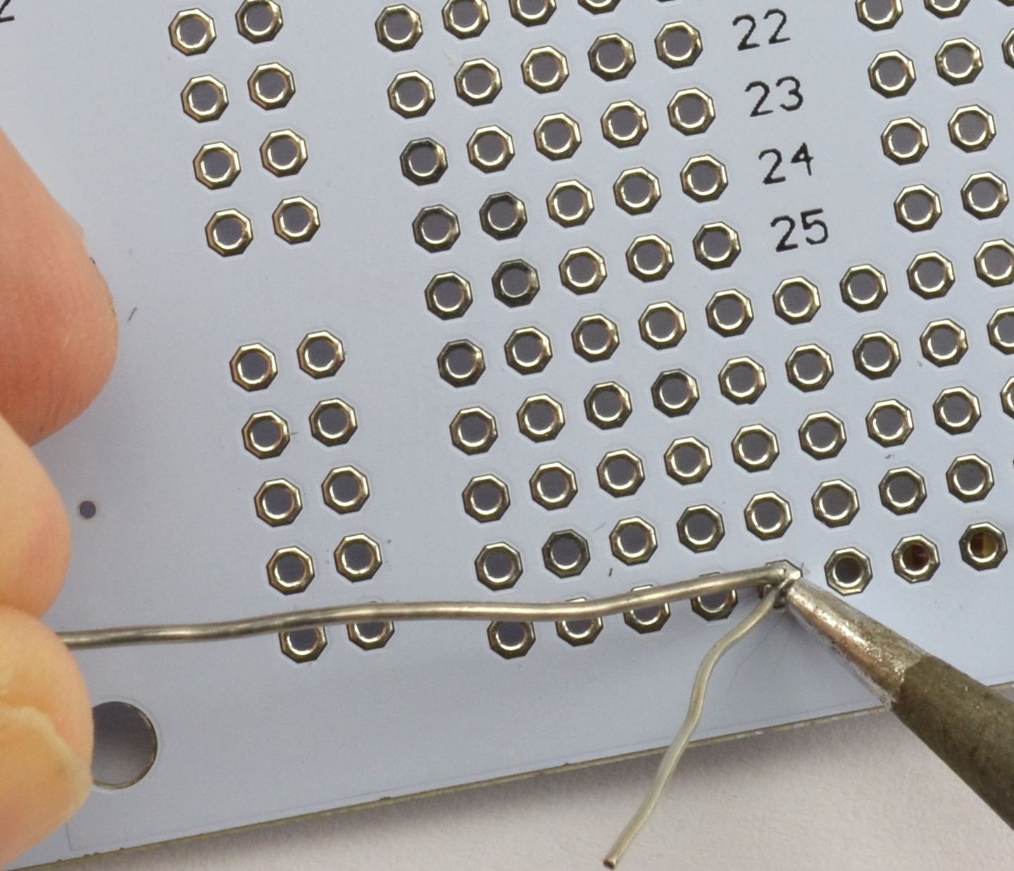
Figure 20-15. Soldering a Circuit Board Joint
In more detail, to make a good solder joint, you should:
- Make sure your iron is up to temperature for the solder you are using. For leaded solder, that should be around 280°C (536°F) and for unleaded solder 310°C (590°F). If things aren’t working well try altering the temperature.
- Clean the tip of your iron on a damp sponge or brass wool. It should look shiny when you are done.
- Touch the iron to where the component lead meets the solder pad and leave it there for just a second or so to heat.
- Feed in some solder to where the circuit board and component lead meet until the solder has flown around the lead covering all the pad, with a little peak of solder pulled up toward the top of the lead.
- Cut off the excess lead.
Safe Soldering
Soldering irons get hot—very hot—and can inflict nasty burns, so be careful. Safety glasses are a good idea as occasionally specks of solder can fly off if flicked by a lead, or even from boiling flux, and if your eyes are close to the thing you are soldering (which is quite likely) you could damage your eyes.
It is also a good idea to use a fume extractor (these do not need to be expensive; see Appendix A) to take away the noxious fumes released as the flux in the solder burns. This is not really something you want in your lungs.
Discussion
Due to various international regulations that have been put in place, lead (the element Pb) is rapidly being phased out of use in circuit board manufacture. Most solder is now unleaded. Unfortunately, unleaded solder has a higher melting point and is generally a bit more difficult to use than the leaded variety. You can still buy leaded solder and many people keep a reel of “the good stuff.”
If you are using small components, then use a thin multicore rosin solder. I use 0.7mm.
See Also
You will find some good video tutorials for soldering on YouTube, and SparkFun has a great video on how to solder here: http://bit.ly/2mDxVyD.
I also recommend the book Learn to Solder by Brian Jepson, Maker Media, 2012.
20.5 Explore Surface-Mount Soldering
Solution
If you are making a one-off, or just a few prototypes, consider soldering by hand. Unless you are very skilled, the results will not be great, but you should be able to make a functional prototype this way.
Soldering by hand is a great deal easier if you stick to SMD resistors and capacitors that are 0603 or larger and ICs with a pin spacing of 50 mils (1.27mm) or wider as found in SOIC packages.
Most components are available in a variety of different package sizes.
When soldering SMDs you will need to hold the part down (I use tweezers) while you solder each pin to a pad. As with through-hole soldering, heat the pin and pad for a second or so before touching the solder onto the pad and pin, flowing the solder into the joint.
When soldering the first pin, it’s best to put a tiny blob of solder on one pad (Figure 20-16) and then solder the first pin by just heating and pressing the pin onto the pad (Figure 20-17). You should find that once one pin is soldered, you don’t need to hold the device in place (Figure 20-18). When you have soldered all the other pins, it’s a good idea to circle back to the first pin and just flow a bit of solder into it to make sure it’s well soldered.
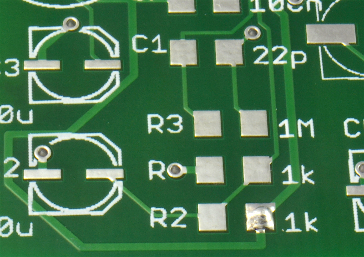
Figure 20-16. Placing a Small Blob of Solder on One Pad
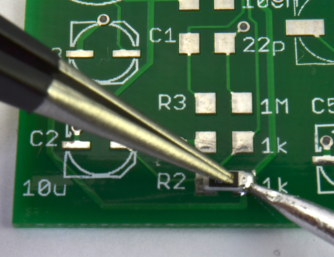
Figure 20-17. Holding the Component in Place While Soldering the First Pin
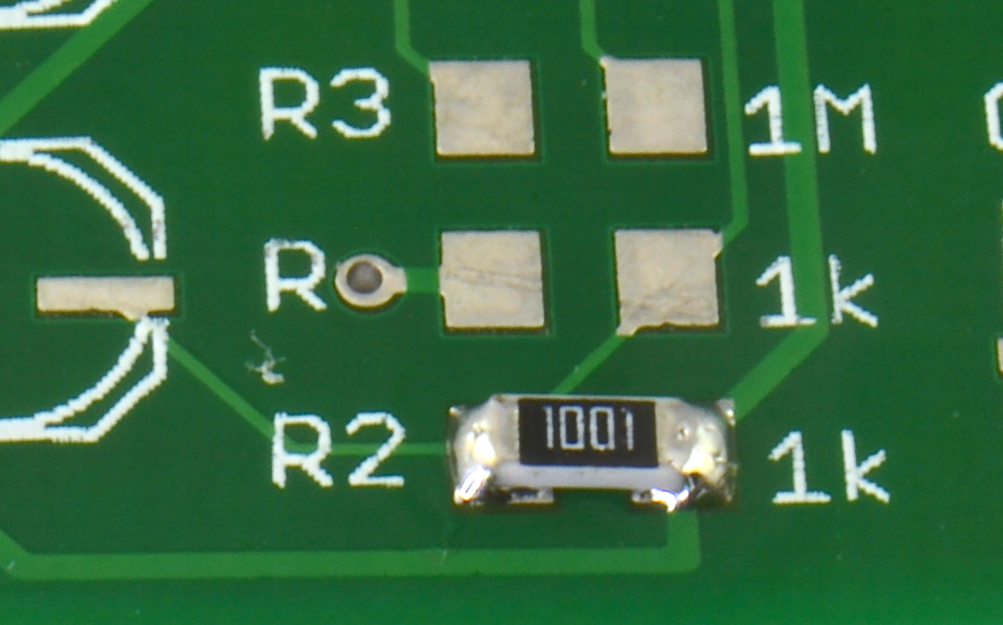
Figure 20-18. A Hand-soldered SMD Resistor
An alternative to using a soldering iron is to use solder paste and a hot-air gun. Here the procedure is to first place a little solder paste onto the component pads (Figure 20-19). Place the component onto the pads and hold it down with the tip of the tweezers while you heat it up with the hot-air gun (Figure 20-20).
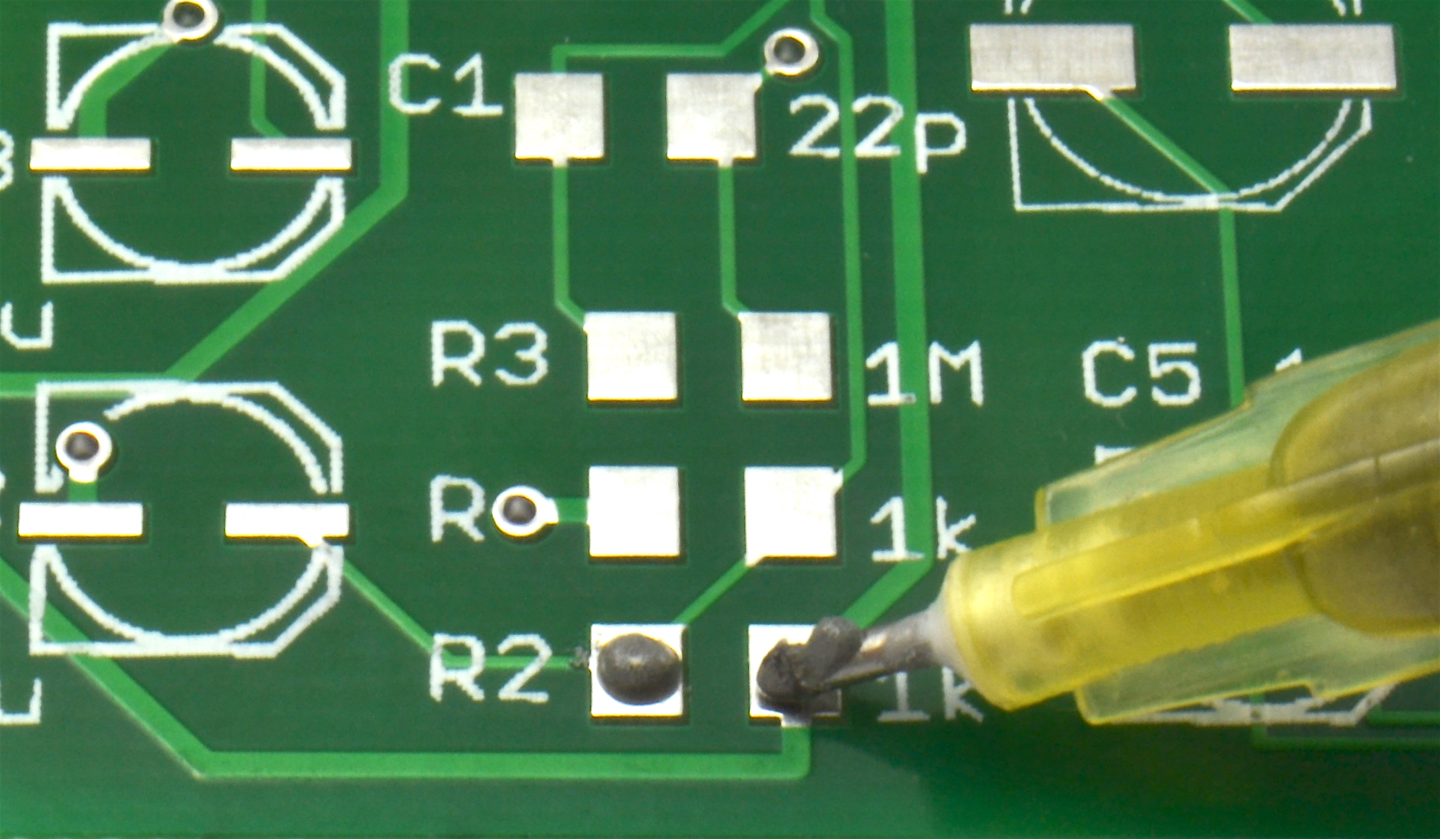
Figure 20-19. Placing a Small Blob of Solder Paste on the Pads
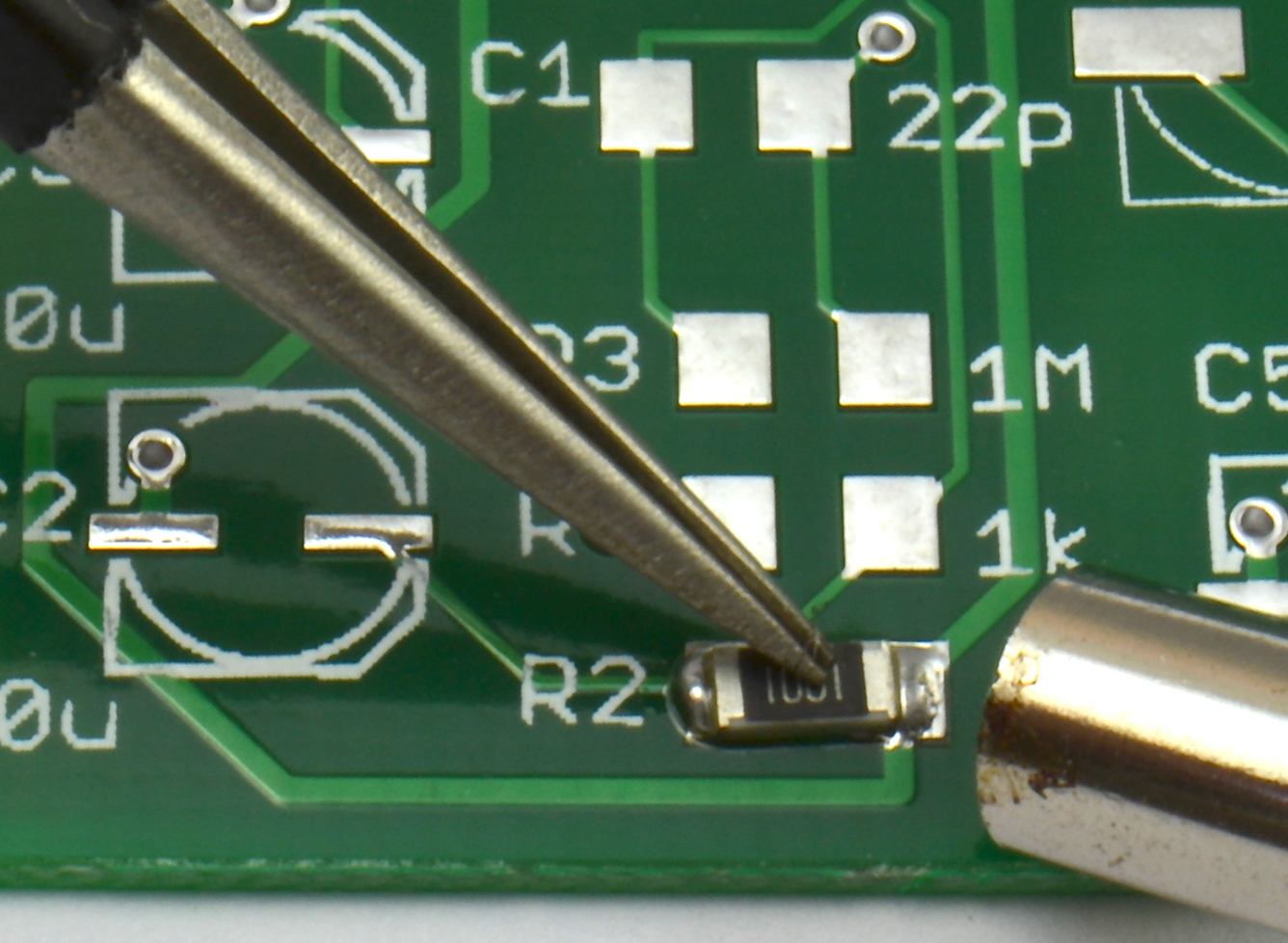
Figure 20-20. Holding the Component Down While Heating with the Hot-air Gun
If you have a reflow oven, like the homemade one shown in Figure 20-21, then you start as you would when using a hot-air gun, placing solder paste onto each pad. This task can be made easier by using a stencil, which most circuit board manufacturers will provide during circuit board manufacture for an extra cost.
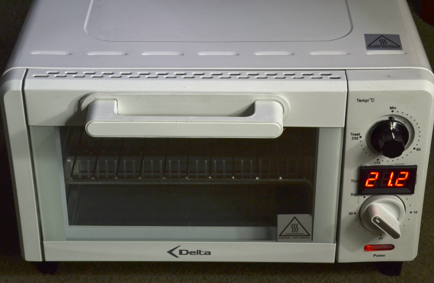
Figure 20-21. A Homemade Reflow Oven
Having applied the solder paste, place the components (they will stick to the solder paste). Then “cook” the board to melt the solder paste. A sophisticated reflow oven will have profiles you can set for different types of solder paste. It is surprising what you can get away with using a homemade oven. Mine is made from a converted toaster oven with a temperature probe fitted. A bit of trial and error will eventually get things right, but, purely as an example, my procedure for using lead solder paste (which has a lower melting temperature) is:
- Place the board in the oven.
- Put the oven on maximum until the temperature reaches 80°C, then turn it off and let it “soak” for 2 minutes during which the reported temperature will continue to increase, peaking at about 130°C.
- Put the oven on maximum again until the solder paste has melted (at about 140°C) and then the oven should be turned off.
- After a further 30 seconds, open the oven door to let the circuit board cool quickly.
Your procedure will no doubt be different, but when you’ve found the magic formula for your setup, it should work every time.
Homemade SMD Ovens Can Cause Fires
Modified toaster ovens are potentially very dangerous (they have the nickname “fire starters” for good reason). Both when making modifications to the oven and when using it you must know exactly what you are doing and the risks involved. If you are not absolutely sure about what you’re doing, do not be tempted to make your own.
A homemade oven should not be left unattended for a moment while in use.
See Also
For soldering through-hole components, see Recipe 20.6.
20.6 Desolder Components
Solution
Desoldering is generally a lot harder than soldering. Unless the component you want to desolder is valuable, you can make your life easier by not worrying about destroying it to get it off the board.
For through-hole two-lead components like resistors, I use the following procedure:
- Remove as much of the solder as possible by pressing the desoldering braid against the pad and then heating it with the soldering iron (Figure 20-22).
- Sometimes this is so effective that you can then just pull out the component, but more often than not you will need to snip the component in half, or cut the lead at one end if there is enough spare lead to get a hold of with a pair of pliers on the top side of the board.
- One leg at a time, hold the lead on the top side of the circuit board with pliers, and pull the lead out while heating the solder joint from below.
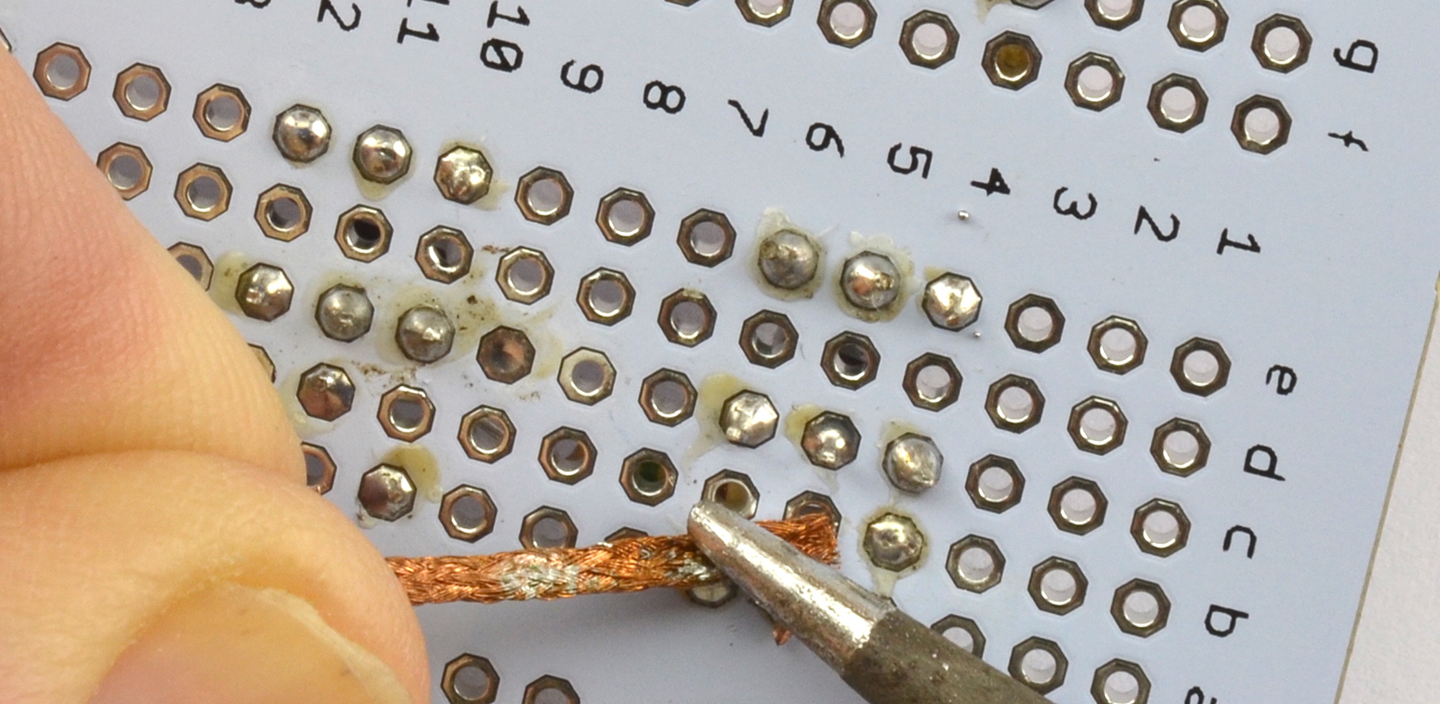
Figure 20-22. Using the Desoldering Braid
Desoldering DIL ICs is a lot more difficult, but again, if you don’t mind sacrificing the IC, you can chop off its pins and desolder each one separately. Removing the IC as a whole is also possible. Starting with the desoldering braid, get the IC as clean of solder as possible and then push a screwdriver under one end of the IC and gently lever it off, swapping sides with the screwdriver to gradually work the IC out.
Desoldering SMDs is much easier. Just hold a hot-air gun over the component and it will probably just blow away after a while.
Discussion
Desoldering components is time consuming and you often end up damaging the circuit board pads or the component being removed. Sometimes it’s quicker just to throw it in the trash and start again.
See Also
To solder through-hole devices, see Recipe 20.4 and for SMDs Recipe 20.5.
20.7 Solder Without Destroying Components
Solution
Determine the power the device will need to continuously dissipate and decide the maximum temperature (Tmax) you want the device to reach (less than its absolute maximum in the datasheet). Then use the following formula to find the thermal resistance the heatsink (RØheatsink) will need to provide:

Here, Tambiant is the ambient temperature and RØpackage is the thermal resistance of the component package (1.5° C/W for a TO220 power transistor).
As an example, the datasheet for a TIP120 states that the maximum temperature is 150°C so let’s stay well under this with a Tmax of 130°C. Let’s assume the TIP120 is expected to be used in a circuit where it will generate 10W of heat.
Let’s also assume the ambient temperature of the project’s enclosure is 30°C (very dependent on ventilation).
Plugging these numbers into the formula, we have:

Searching through the heatsink listings in a component catalog, you can find heatsinks with thermal resistances of 8.5C/W or better.
Discussion
Having done the calculations, test the temperature rise of the device for real and in its final enclosure, as the degree of ventilation in the enclosure will make a big difference. If need be, a fan on the heatsink will increase the heat dissipation considerably.
Heatsinks are available in a great variety of shapes and sizes. Figure 20-23 shows a selection of them.
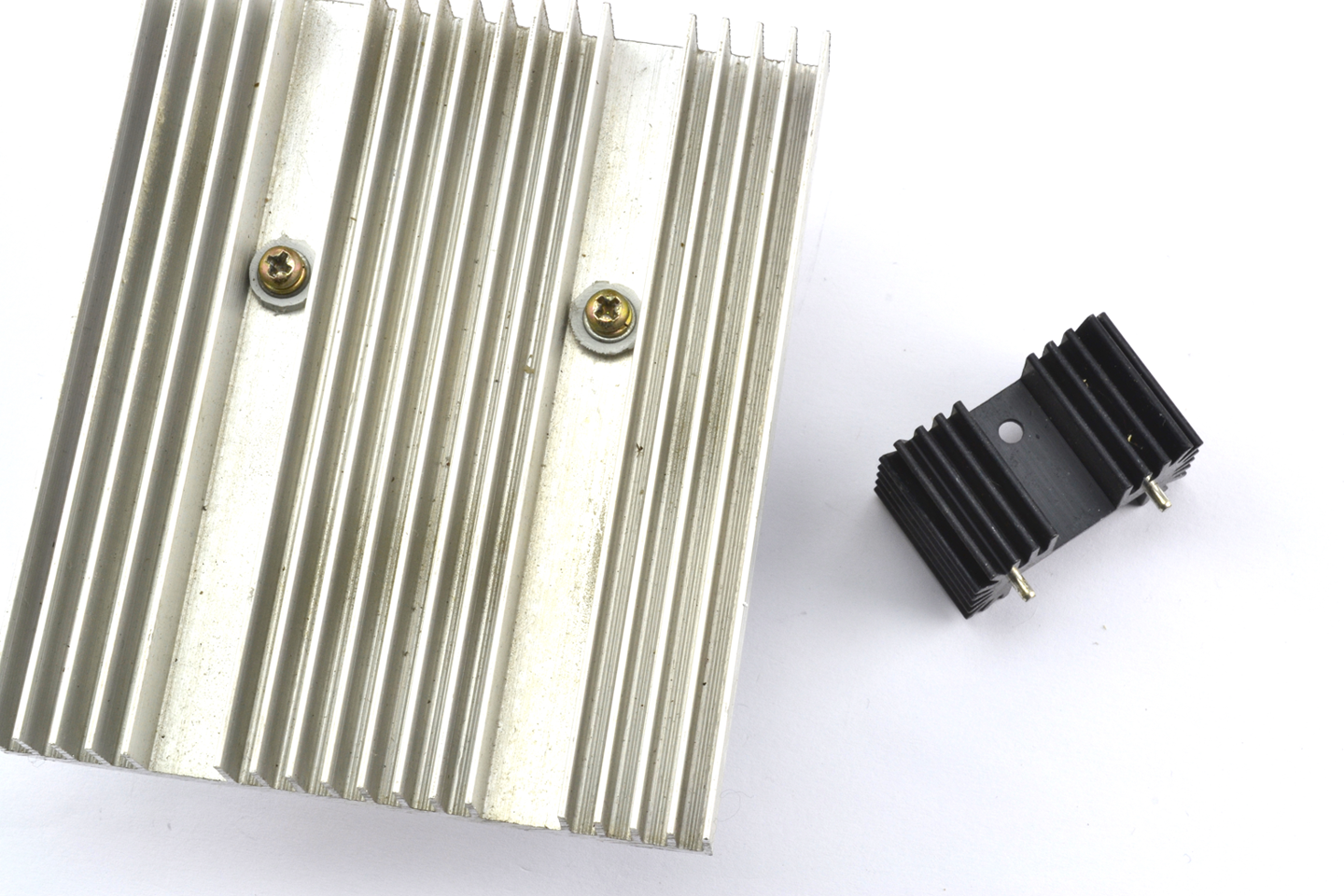
Figure 20-23. Heatsinks (Large and Small)
When attaching a device to a heatsink, you should smear a thin layer of heatsink compound (white paste) onto the device to greatly improve the heat transfer from the device to the heatsink.
See Also
For background on power, see Recipe 1.6.
The datasheet for the TIP120 is found here: http://bit.ly/2mHBQy6.