Table of Contents for
Electronics Cookbook
 Electronics Cookbook
Published by
O'Reilly Media, Inc., 2017
Electronics Cookbook
Published by
O'Reilly Media, Inc., 2017
- Cover
- nav
- Electronics Cookbook
- Electronics Cookbook
- Preface
- Theory
- Resistors
- Capacitors and Inductors
- Diodes
- Transistors and Integrated Circuits
- Switches and Relays
- Power Supplies
- Batteries
- Solar Power
- Arduino and Raspberry Pi
- Switching
- Sensors
- Motors
- LEDs and Displays
- Digital ICs
- Analog
- Operational Amplifiers
- Audio
- Radio Frequency
- Construction
- Tools
- Parts and Suppliers
- Arduino Pinouts
- Raspberry Pi Pinouts
- Units and Prefixes
- Index
- About the Author
- Colophon
Chapter 17. Operational Amplifiers
17.0 Introduction
Operational amplifiers, or more commonly known as op-amps, have a helpful way of making theory easy to implement. If you need to make a filter or preamplifier, an op-amp is often the best solution.
An op-amp has two inputs and one output and is represented in schematic diagrams (Figure 17-1) as a triangle with the output coming from one apex and the two inputs labeled + and – on the opposite side. They also need positive and negative power connections. They are available in a variety of IC packages with 5, 6, or 8 pins. ICs are also available that contain two or four op-amps in a single package.
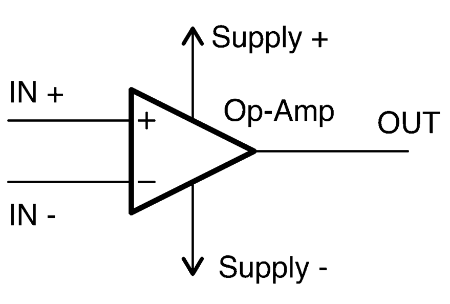
Figure 17-1. Schematic Symbol for an Op-Amp
Op-amps amplify the difference between the + and – inputs. The gain of an amplifier will generally be millions or even billions. So the output voltage may be 1,000,000 times the difference between the input voltages. Such a high gain may sound desirable, but it is actually too high to do anything useful with. To reduce the gain to a more manageable level, an op-amp is almost always used with negative feedback where some of the output is fed back to the negative input. You will find examples of using feedback in this way in Recipe 17.4 and Recipe 17.5. In Recipe 17.6 you will see how if all of the output is fed back to the negative input the output will follow the positive input to the op-amp rather like the emitter-follower described in Recipe 16.4.
Traditionally op-amps are powered with a split power supply that has positive and negative supply voltages (Recipe 17.2) in addition to GND in the middle. However, the prevelance of microcontrollers with single 3.3V or 5V supplies has led to many op-amps being capable of single-supply operation (Recipe 17.3).
An op-amp IC is much better than a discrete-transistor design in most situations, providing a lower component count and generally excellent performance. Special types of op-amps are available for different power supply, frequency, and noise requirements.
17.1 Select an Op-Amp
Solution
Here I have tried to simplify this enormous choice to a small set of readily available devices to suit all applications.
Factors that you need to consider include:
- Price
- Power supply range
- Whether you need the outputs and inputs to be able to reach the full supply range (rail to rail)
- Speed. The gain bandwidth product is the frequency at which the gain of the op-amp (without any feedback) will drop to 1.
- Output slew rate. The maximum rate at which the output can increase.
- Common mode rejection (CMR). A op-amp amplifies the difference between its two inputs, and the CMR of an op-amp is the degree to which any simultaneous changes to both inputs are ignored. This is measured in decibels (see Recipe 16.11).
- Noise. All electronic circuits generate a small amount of noise. This can cause problems with very weak signals, so sometimes in high gain applications low-noise op-amps are necessary.
- Supply current. Some op-amps operate at such low currents that they are suitable for long-term battery use. Some op-amps also have a power-down or standby mode that allows them to be virtually switched off. For example, a microcontroller might do this before putting itself to sleep to save battery power.
- Output current. Sometimes a high output current from an op-amp can be useful to directly drive a small load.
- Number of op-amps per package. Op-amps are available in packages that contain 1 to 4 op-amps in a single package. If you have a circuit that uses multiple op-amps, this can save space and money in your design.
A good selection of devices to start from are listed in Table 17-1.
| LM741 | LM321 | TLV2770 | OPA365 | |
|---|---|---|---|---|
| Description | Perhaps the longest-lived and most popular op-amp. | A good high-supply voltage device capable of single-supply operation. | A single-supply low-voltage device with a standby, low-current mode. | A high-performance, low-voltage, low-noise device. SMD only. |
| Guide cost | $0.50 | $0.70 | $2 | $2 |
| Supply voltage range | ±10–22V | 3–30V | 2.5–5.5V | 2.2–5.5V |
| Rail to rail | N | N | Y | Y |
| Gain bandwidth product | 1MHz | 1MHz | 5.1MHz | 50MHz |
| Slew rate | 0.5V/µs | 0.4V/µs | 10V/µs | 25V/µs |
| Common mode rejection | 96dB | 85dB | 86dB | 120dB |
| Noise (nV/√Hz) | Not specified | 40 | 17 | 4.5 |
| Supply current | 1.7mA | 0.7mA | 1mA (1µA standby) | 4.6mA |
| Output current | 25mA | 20mA | 50mA | 65mA |
| Dual-amp package | LM747 | LM358 | TLV2773 | OPA2385 |
| Quad-amp package | LM148 | LM324 | TLV2775 | Not available |
Discussion
There will be times when you need to step out from the selections in Table 17-1 for some particular application. Perhaps you need an op-amp that works at high frequencies, but has a high upper supply voltage. In such cases, there will almost certainly be a device that fits the niche, but to find it, you will need to do some searching on the internet for recommendations and then carefully inspect the datasheets.
Note that not all op-amps have the same pinout. See Appendix A for pinouts for the op-amps described in this recipe.
See Also
Take a look at the datasheets for the op-amps featured in this recipe:
You will also find an op-amp used in Recipe 18.3.
17.2 Power an Op-Amp (Split Supply)
Solution
Use a regulated supply or batteries, or both. In any case, use a linear voltage regulator rather than a switching regulator. The current consumption of an op-amp is low enough that power-supply efficiency does not need to be considered.
If you are operating the op-amp with a split power supply, you can use positive and negative versions of a linear regulator as shown in the ±12V supply shown in Figure 17-2.
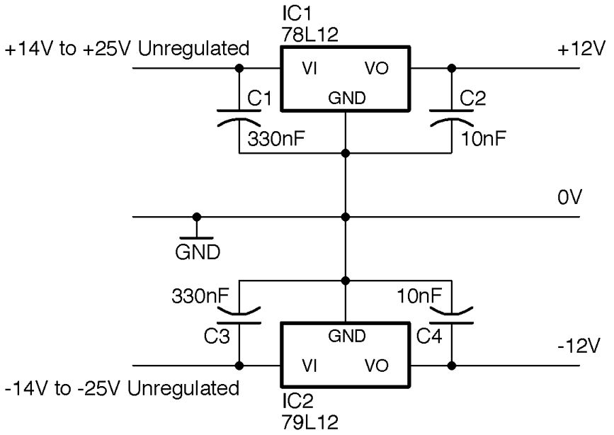
Figure 17-2. A Split 12V Regulated Supply
Op-amps benefit greatly from the use of decoupling capacitors (see Recipe 15.1). If you have an undemanding application, a single 100nF capacitor placed close to the op-amp IC will be just fine. For more demanding applications where you have a lot of gain, it is common to use both a 100nF and 10µF capacitor next to each other and close to the IC body.
Discussion
The positive side of the supply is as described in Recipe 7.4, but in this case, in addition to a 78L12 (L for low-power) to regulate the positive side of the supply, a 79L12 negative voltage regulator is used to regulate the negative side of the supply.
See Also
Although a split supply like this is quite common in audio and scientific instruments, in general, it is more convenient to use a single supply as described in Recipe 17.3.
17.3 Power an Op-Amp (Single Supply)
Solution
Figure 17-3 shows a common way of providing a 5V regulated supply and a 2.5V reference voltage using a voltage divider and capacitor. The capacitor C3 stabilizes the voltage further, making it less likely to be influenced by changes in the current flowing through the reference voltage.
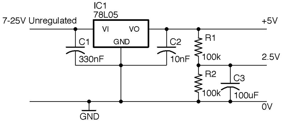
Figure 17-3. Providing a Center Voltage for Single-Supply Operation of an Op-Amp
As you will see in Recipe 17.4 and Recipe 17.5 nearly all op-amp circuits need this middle reference voltage to provide negative feedback to reduce the op-amp’s gain.
Discussion
To improve this and provide a stable center voltage use a voltage divider and capacitor with a unity gain buffer as described in Recipe 17.6. If you have a design that uses several op-amps, you will often find that there is a “spare” op-amp in a quad op-amp package that can be used for this purpose.
See Also
To power an op-amp using a split-voltage supply, see Recipe 17.2.
17.4 Make an Inverting Amplifier
Solution
Connect up your op-amp as shown in the schematic in Figure 17-4, which shows the arrangement assuming a split ±12V supply.
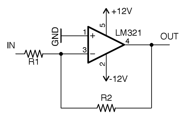
Figure 17-4. An Inverting Amplifier
Without any feedback from the output of an op-amp to its input, the gain of the op-amp will be millions or billions, which is far too high to do anything useful other than amplify noise. This circuit uses R1 and R2 to reduce the gain of the op-amp to a reasonable level. A reasonable level is a factor between 10 and 10,000. If you need more gain than this, you will need to use multiple stages of amplification as well as some filtering to avoid amplifying unwanted noise.
The voltage gain of the circuit is set by the formula:
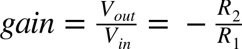
So if we want our amplifier to have a gain of –10 (times 10 but inverted), we could choose a value for R2 of 10kΩ and of R1 of 1kΩ. That way when we put +1V at IN, OUT would have a voltage of –10V. Conversely, if we put –0.1V at IN, OUT would be +1V.
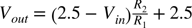
If you want to use a single 5V supply, the same principle applies, but now the amplification takes place relative to the center voltage of 2.5V. Figure 17-5 shows the schematic for using a 5V regulated supply with an OPA365 rail-to-rail single-supply op-amp.
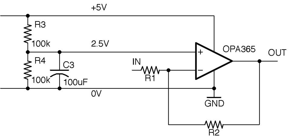
Figure 17-5. Single-supply Inverting Amplification with an Op-Amp
With single-supply operation, the voltage at IN must be between 0 and 5V and the amplification is relative to the center voltage of 2.5V. This means that if the voltage at IN is 2.5V then OUT will also be 2.5V, but if IN is 2.6V (0.1V higher than 2.5V) then OUT will be at 1.5V (1V less than 2.5V).
So, the formula to calculate Vout for any given Vin in the schematic in Figure 17-5 is:
Discussion
No matter what the gain of your amplifier is, the op-amp’s output cannot exceed that of the supply voltages. A rail-to-rail op-amp will allow the voltage to swing from one supply to another but not beyond, but a non–rail-to-rail type op-amp may only allow you to get within a volt or two of the supply voltages.
See Also
Recipe 17.5 shows a noninverting op-amp configuration.
17.5 Make a Noninverting Amplifier
Solution
Use an op-amp in the noninverting configuration of Figure 17-6.
In this case, the gain of the amplifier is given by the formula:
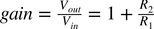
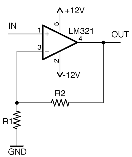
Figure 17-6. A Noninverting Op-Amp Amplifier
If we used a 10kΩ resistor as R2 and a 1kΩ resistor as R1, the gain would be 11. In other words, the voltage at OUT would be 11 times the voltage at IN. If the voltage at IN is negative, the voltage at OUT will also be negative.
In the case of single-supply operation of the amplifier, let’s say 5V, we have the same 2.5V offset to contend with as we did in Recipe 17.4. Figure 17-7 shows how you might build a single-supply noninverting amplifier.
In this case, the gain is still:

And the output voltage is related to the input voltage by the equation:
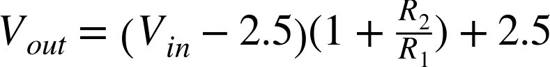
Figure 17-7. Single-supply Noninverting Amplification with an Op-Amp
Discussion
The amplifiers described thus far are capable of amplifying both a DC signal (say from a sensor) and AC-changing signals (perhaps an audio signal). A single-supply 5V (or even 3.3V) design like this is ideally suited to connecting the output to the analog input of a microcontroller, as the voltage can swing between 0V and the supply voltage. In such cases, it is conceptually easier to deal with amplification of a voltage without the added complication of the amplified voltage being inverted about 2.5V, so it is more common to use this noninverting recipe in single-supply designs.
See Also
See Recipe 17.4 for inverting amplifier designs.
17.6 Buffer a Signal
Solution
Configure the op-amp as shown in Figure 17-8.
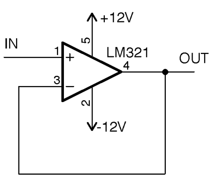
Figure 17-8. A Unity Gain Buffer
The output voltage will track the input voltage. So if the input is 1V, the output will also be 1V. You can then hang whatever load you like off the output, without worrying too much about it affecting the input.
In other words, the voltage is not being amplified but the current that can pass through a load is greatly increased. An example where this might be used is as a headphone amplifier where the signal voltage is high enough in theory to drive the headphones, but the output would not otherwise be sufficient to power the low impedance of the headphones.
Discussion
One situation where a buffer like this can be used is to provide the center voltage for a single-supply op-amp amplifier. Figure 17-9 shows a 5V single supply amplifier modified from Figure 17-7 to use a buffer in this way.
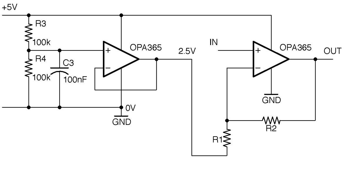
Figure 17-9. Using a Unity Gain Buffer to Provide the Center Voltage for a Single-Supply Noninverting Amplifier
Because the input impedance to the buffer is very high, the value of C3 can be reduced as very little current at all will be flowing out of it. Think of it as reducing ripple on an unloaded power supply.
See Also
Another way to think of the action of a unity gain buffer is as a current amplifier, which is like using a bipolar transistor in an emitter-follower configuration in Recipe 16.4.
17.7 Reduce the Amplitude of High Frequencies
Problem
You want a low-pass filter to reduce the amplitude of high frequencies, but you need it to have a steeper cutoff than the simple RC filter of Recipe 16.3.
Solution
Use an op-amp and a 2-pole filter.
As an example, let’s say we want to revisit the crude filter you saw in Recipe 16.3 designed to separate a 440Hz signal from a 32.7kHz PWM carrier frequency. In that simple RC filter, we ended up with a corner frequency of 1.786kHz and saw that there would be a halving of signal amplitude for each doubling of the frequency. This resulted in a reduction in the amplitude of about a factor of 16 at 32kHz. By using an active filter, the attenuation (fall-off) at 32kHz can be improved to a factor of 100 easily.
When selecting component values for R1, R2, and C2, you can do a whole load of complicated math by hand, or you can use a filter design tool. In this recipe, we will use the Analog Filter Wizard provided by the chip manufacturer Analog Devices available as an online tool at http://www.analog.com/designtools/en/filterwizard/.
When you navigate to that page in your browser, you will be offered the choice of low-pass, high-pass, or band-pass. When you select low-pass, you will be given the opportunity to specify the corner frequency and other parameters for the filter as shown in Figure 17-10.
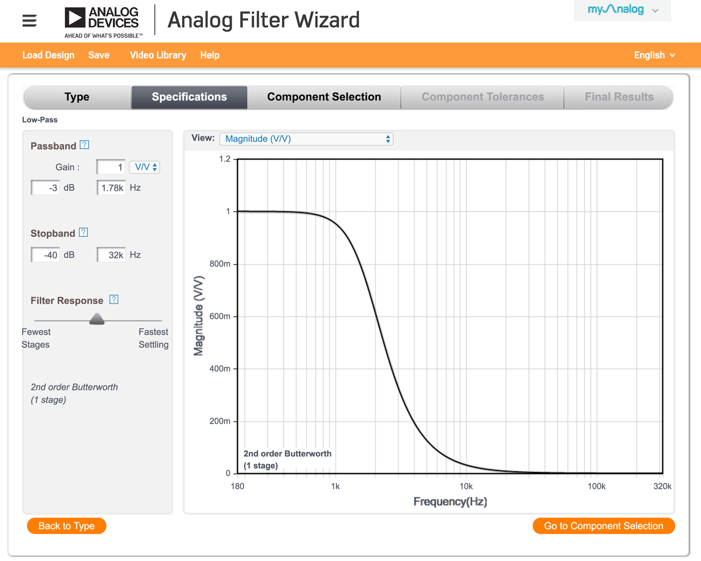
Figure 17-10. Specifying a Filter in the Analog Filter Wizard
The tool is by default configured to work in units of dB (see Recipe 16.11). You can change this to just the amplitude voltage as a ratio by changing the drop-down lists under Passband and next to View to both be V/V as shown in Figure 17-10, where the corner frequency has been set to 1.78kHz and the desired stop-band set to –40dB (factor of 1/100) at 32kHz.
Use the filter-response slider to determine just how steep the curve will be as well as how flat the pass-band’s response is. This will also alter the number of op-amps needed for the design (stages) and the order of the filter. A single op-amp can implement a second-order filter. More orders than that and you will need to chain together several op-amps. The filter type (Butterworth, Chebyshec, or Bessel) will all use the same schematic but different component values to provide different behaviors. See the discussion section for the differences.
For the sake of this example, position the slider so that the second-order Butterworth (first stage) is recommended by the tool and then click Go to Component Selection and “presto,” a schematic complete with component values will be recommended to you as shown in Figure 17-11.
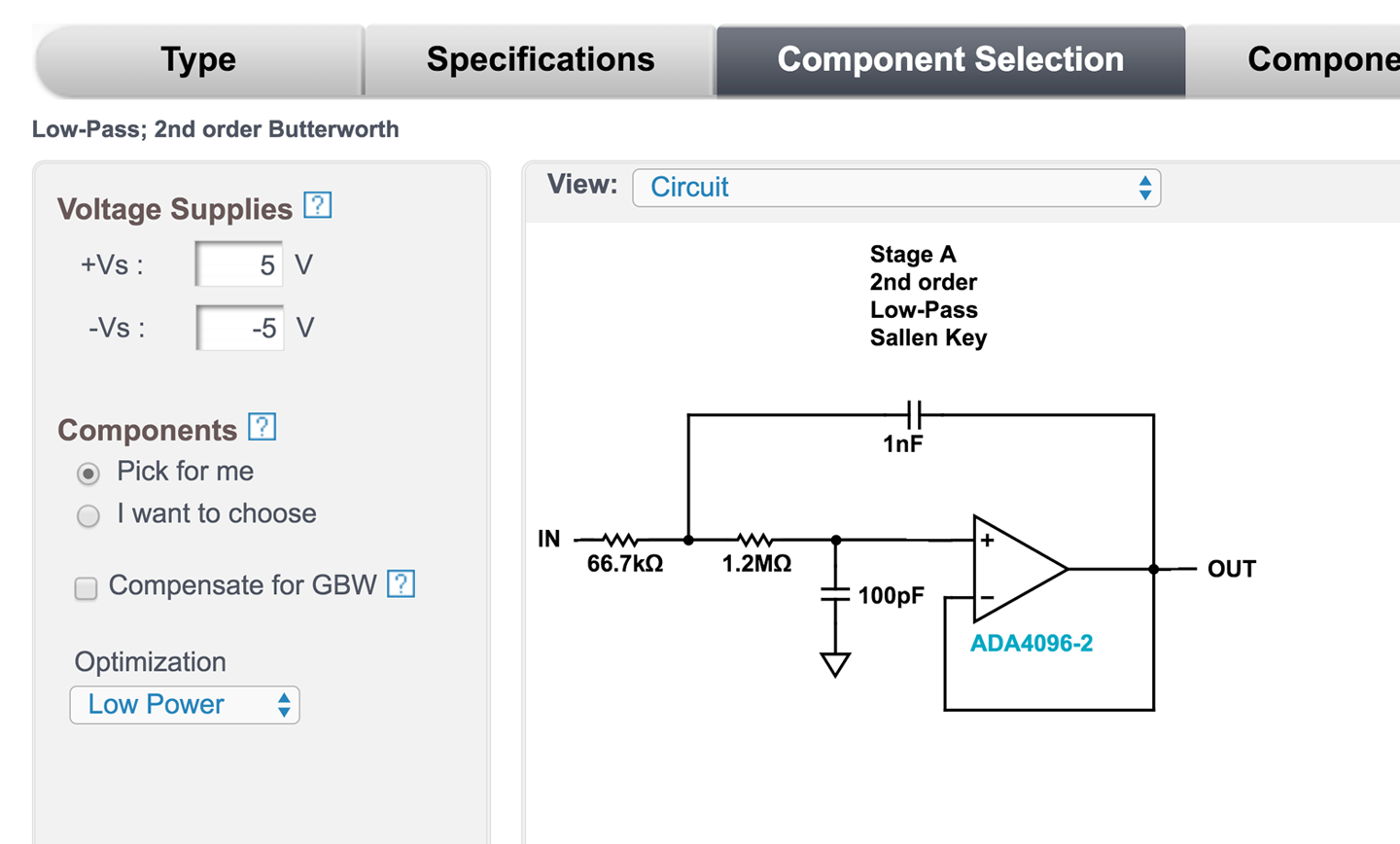
Figure 17-11. Filter Design Complete with Component Values
You can then specify supply voltages and other properties of your design as well as look at the effect of component accuracy on the design. Since this is an Analog Devices tool, it will obviously recommend the op-amps they manufacture, but the designs can be used with other manufacturers’ op-amps.
There is nothing to stop you from adding some gain to your filter so that it both filters and amplifies by replacing the connection from the op-amp output to the negative input with a pair of resistors as used in the noninverting amplifier design of Recipe 17.5. In fact, the design tool does allow you to specify a gain when you are specifying the filter (see Figure 17-10).
Discussion
Unless you have a particularly demanding project, a second-order filter using a single op-amp will generally provide a good balance between complexity and performance. There are whole books written on filter design and other more complex filter design tools.
The properties of the three filter types offered by the Analog Filter Wizard are:
- Butterworth
- A very flat response (the gain remains the same) for the pass-band before you get to the corner frequency, but the transition from pass-band to stop-band is not as steep as for other filter types. Butterworth filters introduce a frequency-dependent phase-shift between the input and output signals, which leads to distortion of the original signal.
- Chebyshev
- Has some gain ripples in the pass-band, but provides a much steeper transition from pass-band to stop-band, although it also suffers from phase-shift.
- Bessel
- Has very little phase-shift at the expense of an even less steep transition from pass-band to stop-band.
These types are all implemented using the same schematic in Figure 17-11; the calculations performed by the Analog Filter Wizard determine the type of filter.
See Also
For other types of filter designs, see the next few recipes.
17.8 Filter Out Low Frequencies
Solution
Use a second-order filter implemented using a single op-amp and design it using a design tool such as the Analog Filter Wizard. Figure 17-12 shows the frequency response of a filter designed by the Analog Filter Wizard to provide high-pass filtering with a gain of 10 and a corner frequency of 1kHz.
Notice that there is a little “hump” in the response between 2kHz and 3kHz where the gain goes above the desired value of 10. This is called overshoot and is another characteristic of Chebyshev filters.
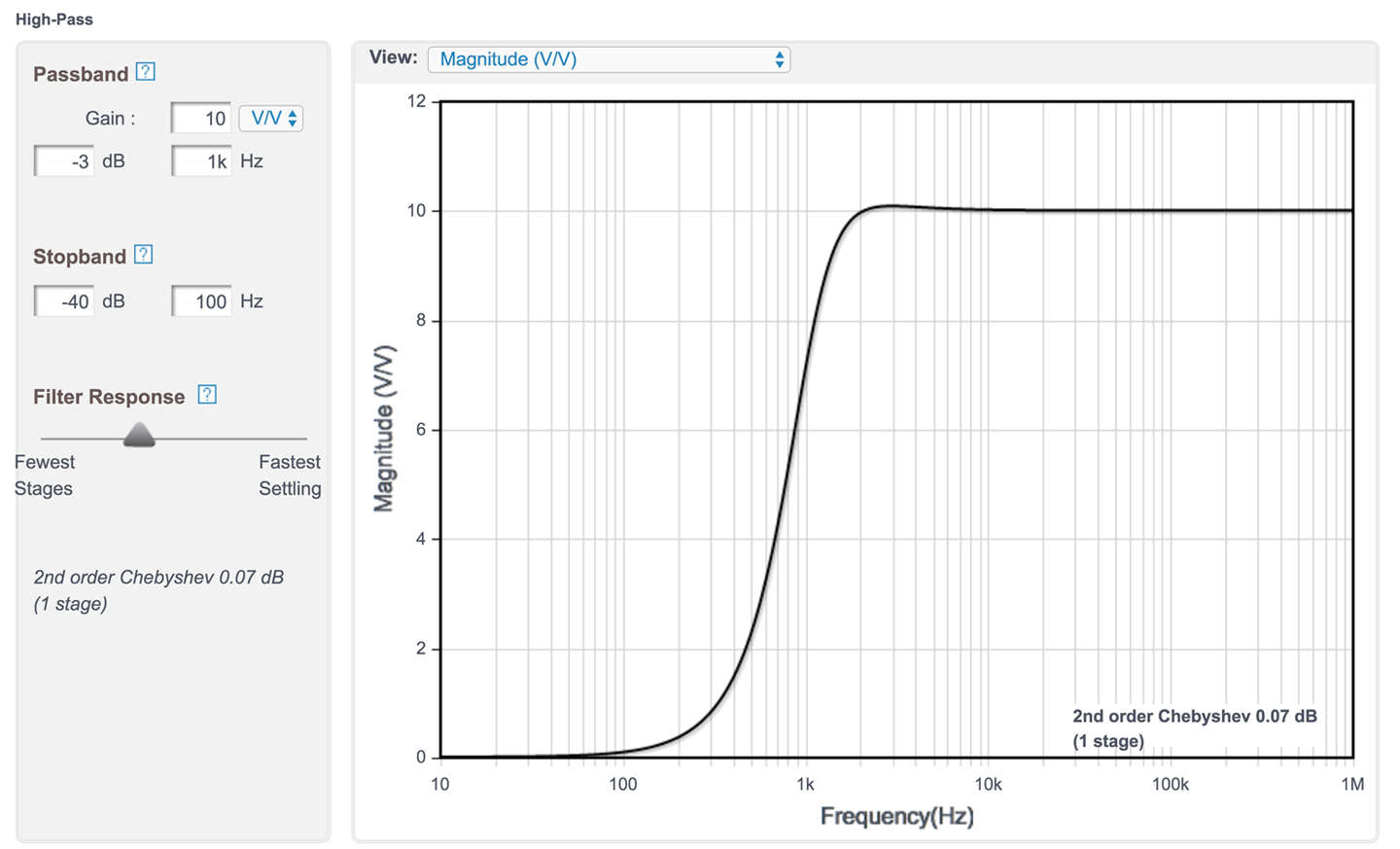
Figure 17-12. Frequency Response of a Second-Order Chebyshev High-pass Filter
The corresponding schematic for this filter is shown in Figure 17-13.
Discussion
Most of the things said in the discussion section of Recipe 17.7, especially about the different types of filters, apply equally well to high-pass filters.
Notice that in Figure 17-13 the Analog Filter Wizard has also helpfully suggested the necessary bypass capacitor values (Recipe 15.1).
See Also
For a low-pass filter see Recipe 17.7 and for a band-pass filter see Recipe 17.9.
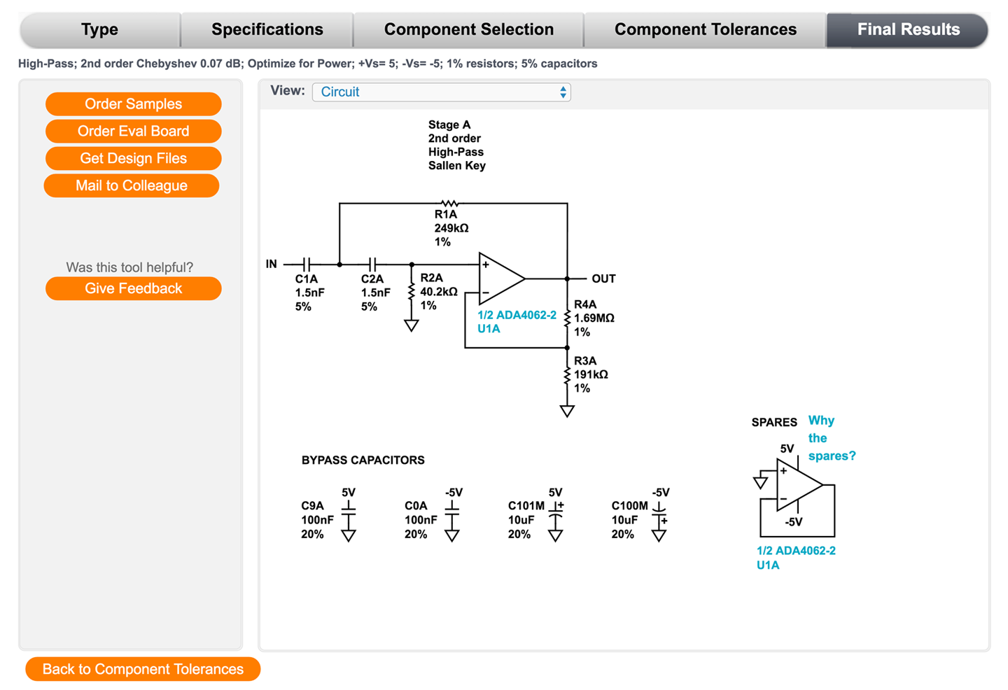
Figure 17-13. Schematic of a Second-Order Chebyshev High-pass Filter
17.9 Filter Out High and Low Frequencies
Solution
If the band of frequencies you are interested in is reasonably wide, then the best solution is to simply pass the signal through a low-pass filter (Recipe 17.7) and then a high-pass filter (Recipe 17.8.) This will require two op-amps, but then dual op-amp ICs are not much more expensive than single op-amp ICs.
Figure 17-14 shows the schematic for a band-pass filter with corner frequencies of 20Hz and 20kHz, which might be used to restrict a signal to the audio-frequency range.
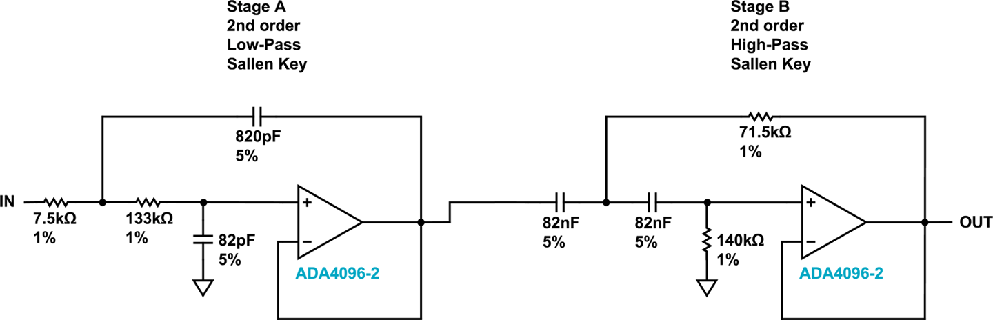
Figure 17-14. A Band-Pass Filter
The filter was designed using the Analog Filter Wizard used in Recipe 17.7 and Recipe 17.8. This time the filter type of Band-pass is selected and the parameters entered as shown in Figure 17-15.
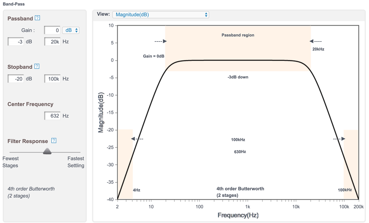
Figure 17-15. Designing a Band-pass Filter Using the Analog Filter Wizard
The pass-band is set to 20kHz for a 3dB drop in amplitude (0.71 of the original amplitude) and the stop-band to 100kHz at the high end where we are aiming for attenuation of 20dB (0.1 of original signal amplitude).
The center frequency is not the 10kHz that you might expect but rather the square root of the product of the upper- and lower-corner frequencies. In other words:

Discussion
Filter design is a specialized field, and in this book, there is only room to look at the most common electronics recipes. However, for many applications a simple design that uses a single op-amp stage will be perfectly adequate.
See Also
For low-pass active filter design see Recipe 17.7 and for high-pass filter design see Recipe 17.8.
17.10 Compare Two Voltages
Solution
Use a device closely related to the op-amp called a comparator. Figure 17-16 shows how you could make a simple automatic light that turns on an LED when the light level falls below a certain threshold.
R1 and R3 form a voltage divider whose output corresponds to the light level; that is, the higher the volate, the higher the light level. The variable resistor R2 is used to set the reference voltage at IN–.
The output of the LM311 provides optimal flexibility by providing connections to both the emitter and collector of the NPN output transistor.
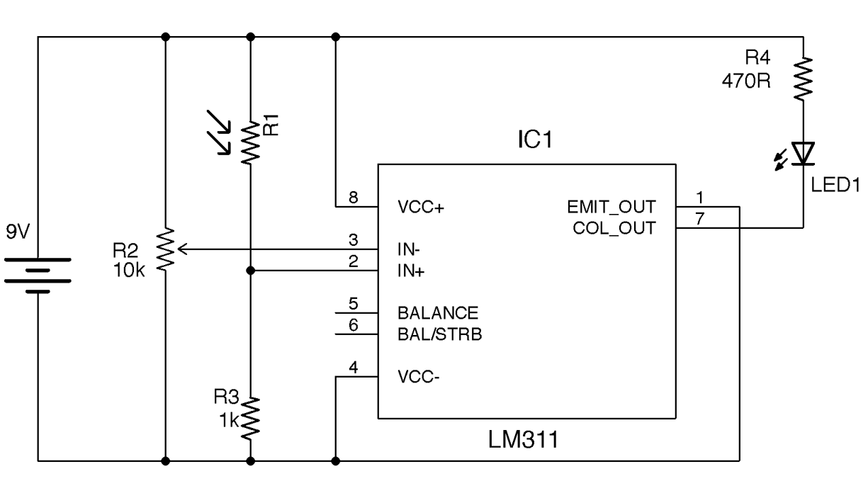
Figure 17-16. Using a Comparator to Control an LED
If the light level is low enough for IN+ to be lower than IN– the base of the output transistor is supplied with current, and since the emitter is grounded, the transistor turns on and current flows through the LED.
This logic of the transistor being on if IN+ is lower than IN– would seem to be counterintuitive, but the output transistor will often have its emitter grounded and the logic output taken from the collector, which is pulled up to VCC. This effectively acts as an inverter and hence the collector output will be high if IN+ is greater than IN–.
See Also
To sense light using an Arduino, see Recipe 12.3 and for a Raspberry Pi Recipe 12.6.