Table of Contents for
Electronics Cookbook
 Electronics Cookbook
Published by
O'Reilly Media, Inc., 2017
Electronics Cookbook
Published by
O'Reilly Media, Inc., 2017
- Cover
- nav
- Electronics Cookbook
- Electronics Cookbook
- Preface
- Theory
- Resistors
- Capacitors and Inductors
- Diodes
- Transistors and Integrated Circuits
- Switches and Relays
- Power Supplies
- Batteries
- Solar Power
- Arduino and Raspberry Pi
- Switching
- Sensors
- Motors
- LEDs and Displays
- Digital ICs
- Analog
- Operational Amplifiers
- Audio
- Radio Frequency
- Construction
- Tools
- Parts and Suppliers
- Arduino Pinouts
- Raspberry Pi Pinouts
- Units and Prefixes
- Index
- About the Author
- Colophon
Chapter 16. Analog
16.1 Filter Out High Frequencies (Quick and Dirty)
Solution
In these circumstances, a simple RC filter (Figure 16-1) will suffice to remove most of the unwanted high-frequency PWM carrier.
Intuitively, all the resistor and capacitor do is make the output slow to respond to changes to the input. All that remains is to decide on suitable values for R and C. We can illustrate this with an example.
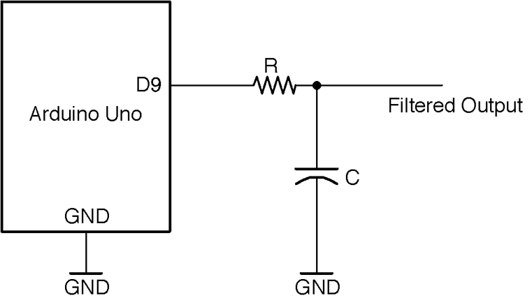
Figure 16-1. Low-pass Filtering of an Arduino-generated PWM Signal
The Arduino Mozzi library (Recipe 18.1) generates PWM (Recipe 10.13) audio output. The length of the pulses on the constant PWM frequency of 32.7kHz determine the amplitude of the lower frequency underlying the audio signal (440 Hz). Figure 16-2 illustrates this.
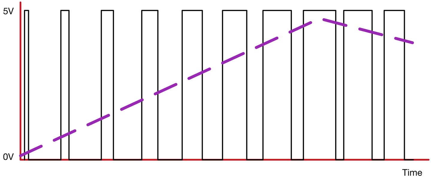
Figure 16-2. PWM of an Audio Signal
The average output voltage is shown by the dashed line, which increases as the pulses lengthen.
Using a value of 270Ω for R and \330nF for C produces the filtering shown in Figure 16-3. The top trace shows the filtered output and the bottom trace the PWM signal.
You can see that the original sine wave from (top) has been extracted from the PWM signal (bottom).
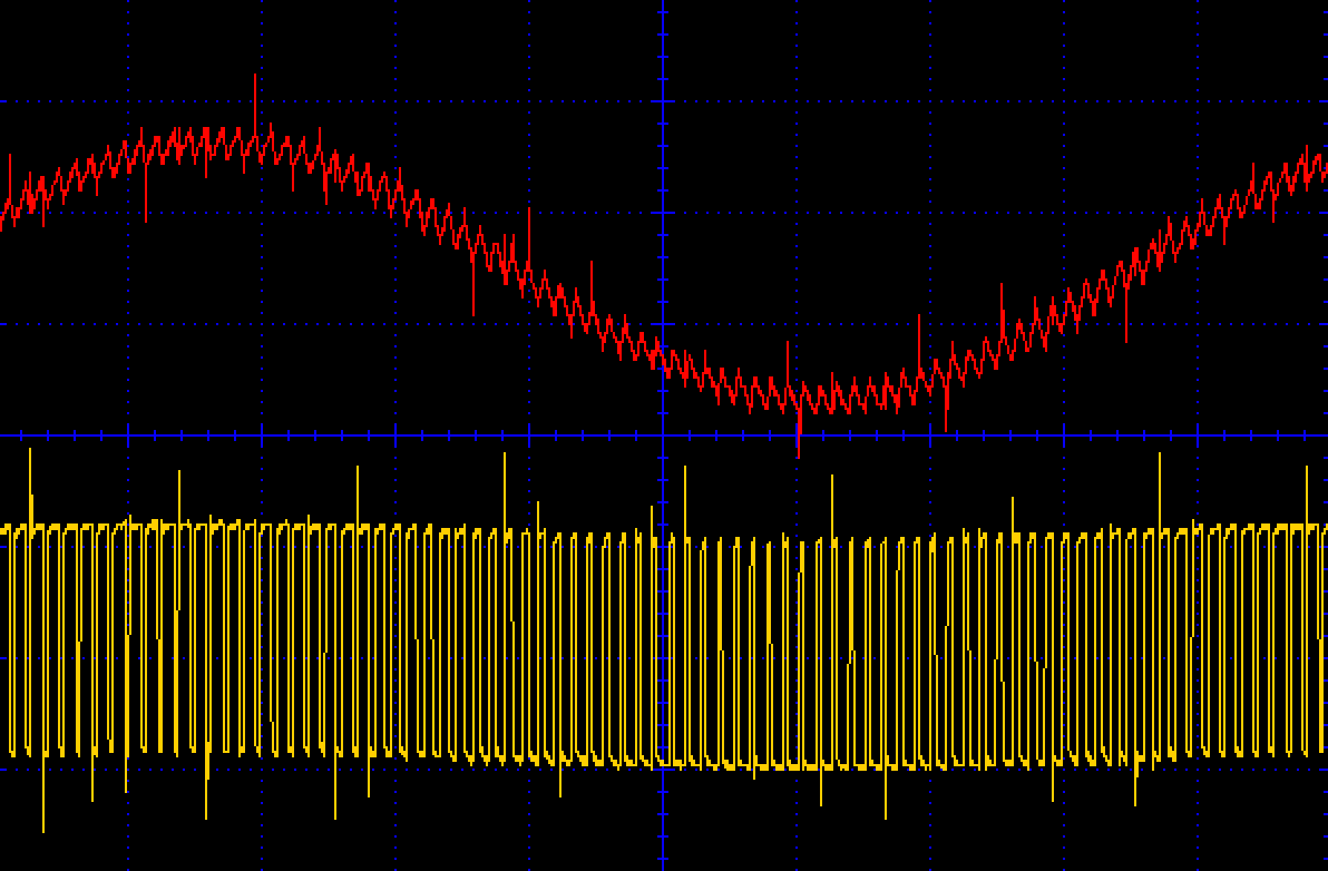
Figure 16-3. Low-pass Filtering of a PWM Signal
Discussion
The kind of RC filter used here is called a first-order filter and only really works well if the signal being filtered is much greater than the frequency you want to keep. Figure 16-4 shows the characteristic plot of gain against frequency.
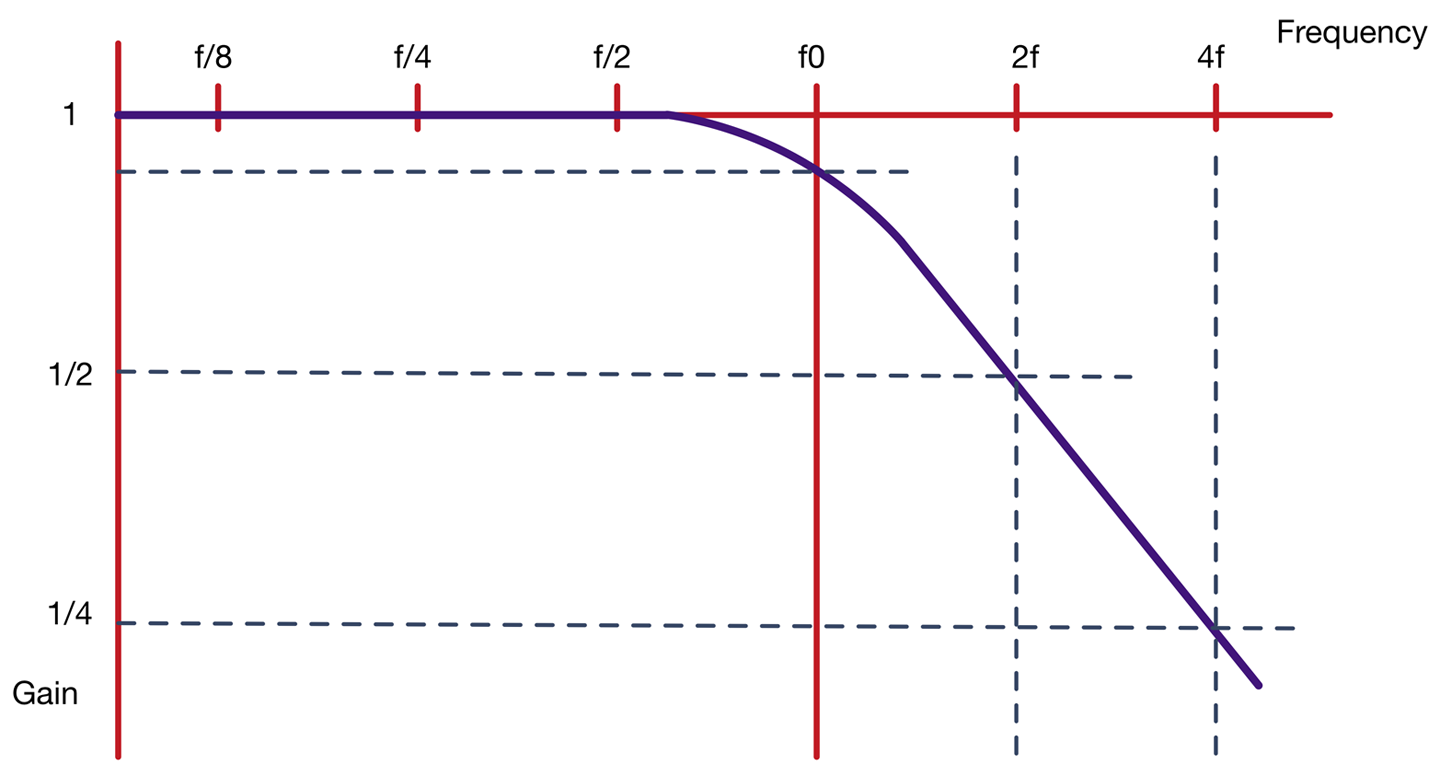
Figure 16-4. A Low-pass Filter’s Frequency Response
A gain of 1 means the signal is unchanged in magnitude. In the “stop band” where the signal is being attenuated, the signal’s amplitude halves every time the frequency doubles.
The start of the stop band is taken to be after the “corner frequency” (f0), which is defined as the frequency at which the signal amplitude has been reduced to 75% for its original value.
The corner frequency is given by the formula:
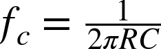
Using a resistor of 270Ω and 330nF capacitor the corner frequency is:

With a corner frequency of 1.768kHz and a frequency of 32.7kHz for the PWM signal (that we are trying to filter out) a quick check will show you that you are looking at a little over four doublings of 1.786kHz, which gives a reduction of four halvings of the amplitude of that high-frequency component. This will reduce the amplitude of the 32.7kHz signal to about 1/16 of its unattenuated value, which is why the PWM frequency is still visible on top of the 440Hz sinewave shown in Figure 16-3.
If you want to try out this experiment, then install the Mozzi library into your Arduino IDE by downloading the ZIP for the library from GitHub and then installing the ZIP for the library from the Arduino IDE’s menu (Sketch→Include Library→Add .ZIP Library).
From the Arduino IDE’s example menu, upload Files→Examples→Mozzi→Basics→Sinewave onto your Arduino and wire it up as shown in Figure 16-1.
Attaching an oscilloscope to the unfiltered and filtered outputs of D9 should give you a trace similar to Figure 16-3.
See Also
For a better-quality filter with a much steeper fall-off of gain with frequency, see Recipe 17.7.
In this recipe, we have talked about attenuation of a signal’s amplitude in terms of halving or quartering. The more common unit for attenuation and amplification of a signal is the dB (decibel). This is described in Recipe 17.1.
A great way to help design filters is to use simulation. This example is used in Recipe 21.11.
For instructions on using an oscilloscope, see Recipe 21.9.
16.2 Create an Oscillator
Solution
Use the transistors in the arrangement shown in Figure 16-5. This arrangement is also sometimes called an “astable,” meaning it has no stable state, and instead oscillates between two states.
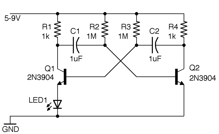
Figure 16-5. A Two-transistor Oscillator
When power is first applied to the circuit both Q1 and Q2 will be off. Very slight differences between the capacitor values and the values of R2 and R3 mean that one of the capacitors will start to charge through R2 or R3 faster than the other. The faster-charging capacitor will win the race to turn on the transistor whose base it is connected to. Current flows through this transistor turning on the LED and drops the collector voltage allowing the slower capacitor to start charging until the opposite transistor turns on and so on.
Discussion
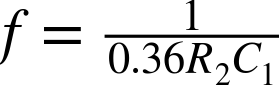
The frequency of this oscillator is determined by the time constant of C1 and R2 (C1 and C2 should have the same value, as should R2 and R3), but also depends on the characteristics of the transistor. For the circuit shown in Figure 16-5 and a supply voltage of 9V, the frequency was measured as 2.8Hz, implying that the frequency is related to R2 and C1 by the formula:
See Also
For an oscillator that uses the NE555 timer IC, see Recipe 16.5.
You can see a video of this circuit in action here: https://youtu.be/-NvMFmPHc4s.
16.3 Flash LEDs in Series
Solution
Build a ring oscillator using MOSFETs as shown in the schematic in Figure 16-6.
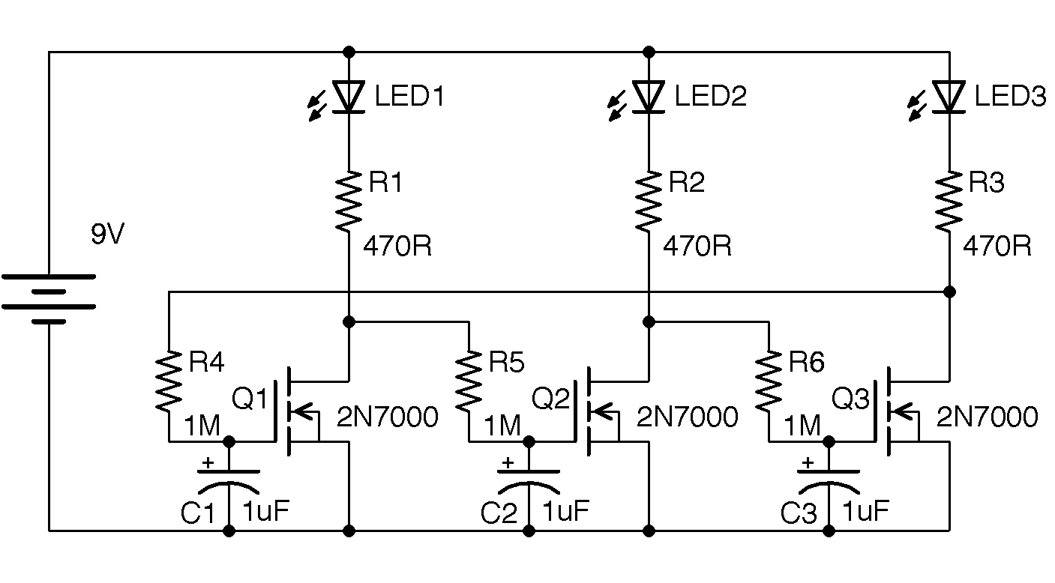
Figure 16-6. A Ring Oscillator
The way to understand how this circuit works is to think of each transistor stage as an inverter. That is, if the gate of the transistor is low, then the drain of the transistor will be pulled high by the LED and resistor. As the transistor’s associated gate capacitor charges, the gate voltage will gradually rise until the transistor is on and then the drain will go low. The final inverter stage then feeds back to the first transistor and the cycle continues. This does not work with an even number of stages as the outputs of the first and last stages would both be high and low (in phase) with each other and no oscillation would occur.
Discussion
This oscillator produces quite a mesmeric effect as the LED brightness gradually increases and decreases.
In practical terms, when considering a large number of LEDs, you would probably use a microcontroller with LEDs attached to digital outputs, or a decade counter like the 4017 described in Recipe 15.6.
See Also
For an interesting Wikipedia article on the ring oscillator, see https://en.wikipedia.org/wiki/Ring_oscillator.
There is a video of this circuit here: https://youtu.be/9O5Ojhr0oGg.
16.4 Avoid Drops in Voltage from Input to Output
Solution
Use a BJT arranged as an emitter-follower, as shown in Figure 15-7. In this case, the input is provided by a pot. The output voltage will follow the input voltage (less the base-emitter voltage).
On the face of it, this may seem pointless and you might be asking yourself why you wouldn’t just take the output from the slider of R1. The reason is that even a very slight load resistance on R1 will alter its output voltage, whereas by using a transistor, a much larger load current can be drawn.
Whatever the voltage set at the base of the transistor (above about 0.6V), the emitter will always be about 0.6V lower, but able to provide significantly more current. In fact, the ratio of base-to-collector current is the DC gain of the transistor. For a transistor like the 2N3904, this is generally taken to be about 100. So for a collector current of say 10mA, less than 100µA should be flowing into the base from R1.
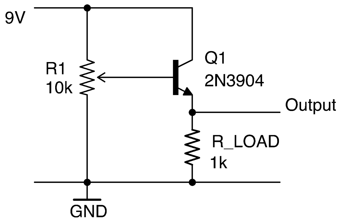
Figure 16-7. An Emitter-Follower Used as a Buffer
Discussion
An emitter-follower like this can be used as the basis of a voltage regulator using the schematic in Figure 16-8, although generally a voltage-regulator IC is an easier option.
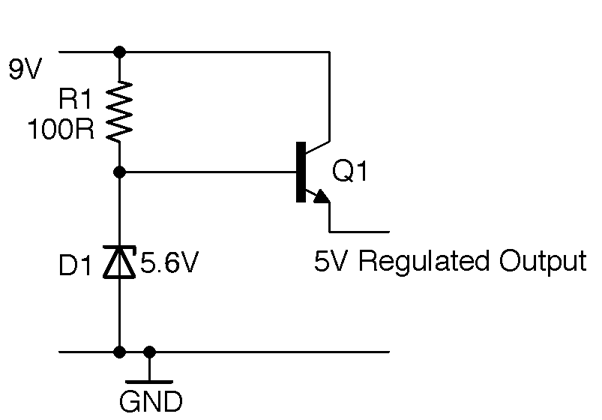
Figure 16-8. A Zener Diode/Emitter-Follower Voltage Regulator
As described in Recipe 4.3 the Zener diode will keep the base of Q1 at 5.6V as long as the input voltage is greater than 5.6V. The Zener diode acts as a voltage reference to Q1, whose emitter will remain at 5V as long as the load current does not become great enough to start drawing significant base current and hence cause the voltage at the base to drop. Using a power Darlington like the TIP120 with its DC current gain of around 10,000 will provide even better regulation, at higher currents, but at the expense of a bigger base-emitter voltage drop (see Recipe 5.2).
See Also
For a more or less perfect unity gain buffer without the base-emitter voltage drop, see Recipe 17.6.
For more information on BJTs, see Recipe 5.1.
16.5 Build a Low-Cost Oscillator
Solution
Use an NE555 timer IC in the configuration shown in Figure 16-9.
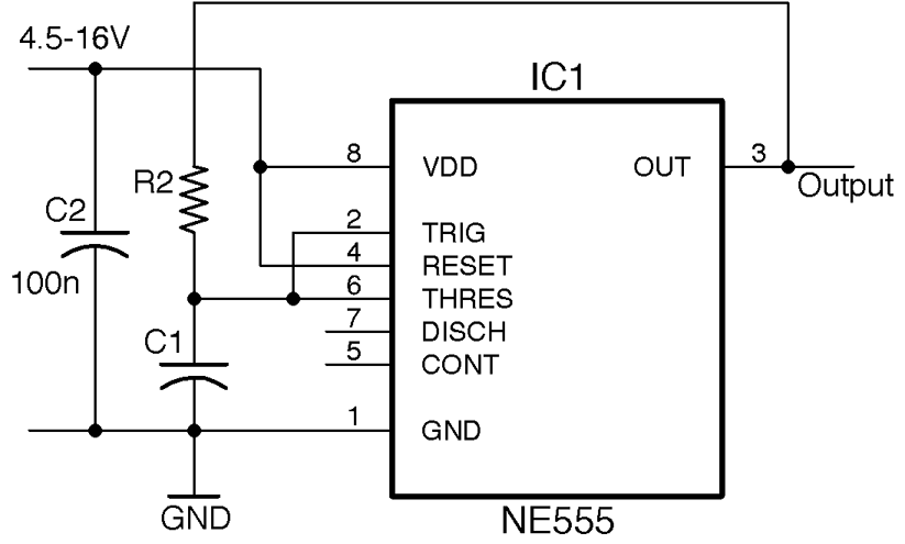
Figure 16-9. An NE555 Oscillator
This is not the standard astable oscillator schematic for an NE555. But unless you need to control the duty cycle for PWM or other purposes, it’s fine for a simple oscillator.
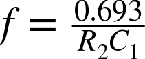
The frequency is set by the values of R2 and C1:
So, for an R2 of 10kΩ and a C1 of 10nF, the frequency is:

To simplify the calculations, standardize a few values of C1. For low-frequency LED blinking, use a 1μF capacitor; for audio frequencies of a few hundred Hz, use 100nF; and for higher frequencies into the kHz, use a 10nF capacitor. Fixing the capacitor in this way means you can use the following formula to calculate the value of R2 that you need:
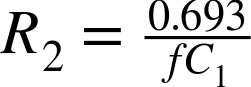
Table 16-1 shows some common frequencies and suitable component values.
| Frequency | C1 | R2 |
|---|---|---|
| 1Hz | 1µF | 693kΩ |
| 2Hz | 1µF | 347kΩ |
| 50Hz | 1µF | 13.9kΩ |
| 100Hz | 1µF | 6.93kΩ |
| 1kHz | 10nF | 69.3kΩ |
| 10kHz | 10nF | 6.93kΩ |
| 100kHz | 10nF | 693Ω |
Discussion
Remember that capacitors in particular are generally only accurate at values of ±10% and the frequency is also somewhat dependent on the supply voltage. Table 16-2 shows the effect of supply voltage on output frequency for this circuit using an R2 of 10kΩ and a C1 of 10nF.
| Supply Voltage (V) | Output Frequency (kHz) |
|---|---|
| 5 | 5.46 |
| 9 | 6.63 |
| 12 | 7.03 |
| 16 | 7.33 |
See Also
You can find the datasheet for the NE555 here: http://www.ti.com/lit/ds/symlink/ne555.pdf.
If you need complimentary outputs from your oscillator, use a 4047 timer IC (Recipe 7.10 ).
The NE555 IC is a versatile device and can also be used as a one-shot timer (Recipe 16.7).
You can also make an oscillator with just two transistors as described in Recipe 16.2.
16.6 Build a Variable Duty Cycle Oscillator
Solution
Use an NE555 timer IC, but this time in the configuration shown in Figure 16-10.
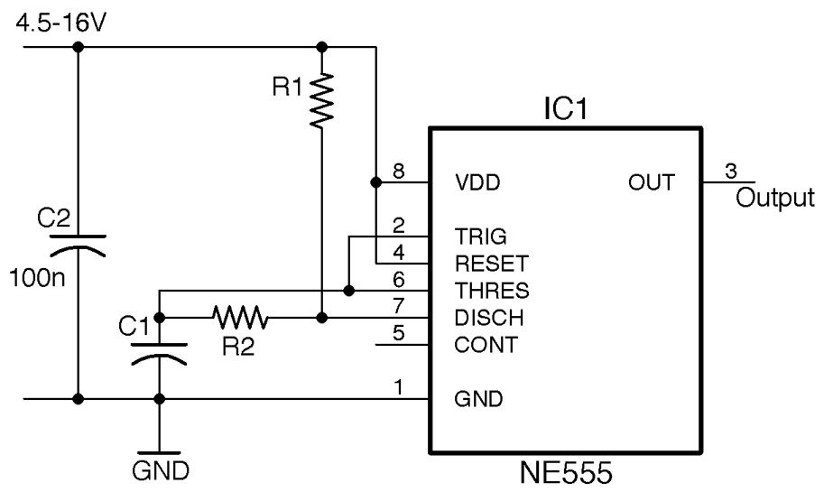
Figure 16-10. An NE555 Oscillator with Adjustable Duty Cycle
The frequency and duty cycle (proportion of the time the output is high to the time it is low) are set by the values of C1, R1, and R2. The period of time the output is high during each cycle is:
The time it is low is given by:

The overall frequency in Hz will be the inverse of these two times added together:
If you want a fairly even duty cycle, you can just use Recipe 16.5, or make sure that R1 is much smaller than R2 (without being 0).
To avoid all the math, there are lots of good online calculators out there you can use. This one is particularly useful as it allows you to enter just the frequency and duty cycle you want.
Discussion
The NE555 timer is an extremely flexible device. Figure 16-11 shows the internal structure of the IC.
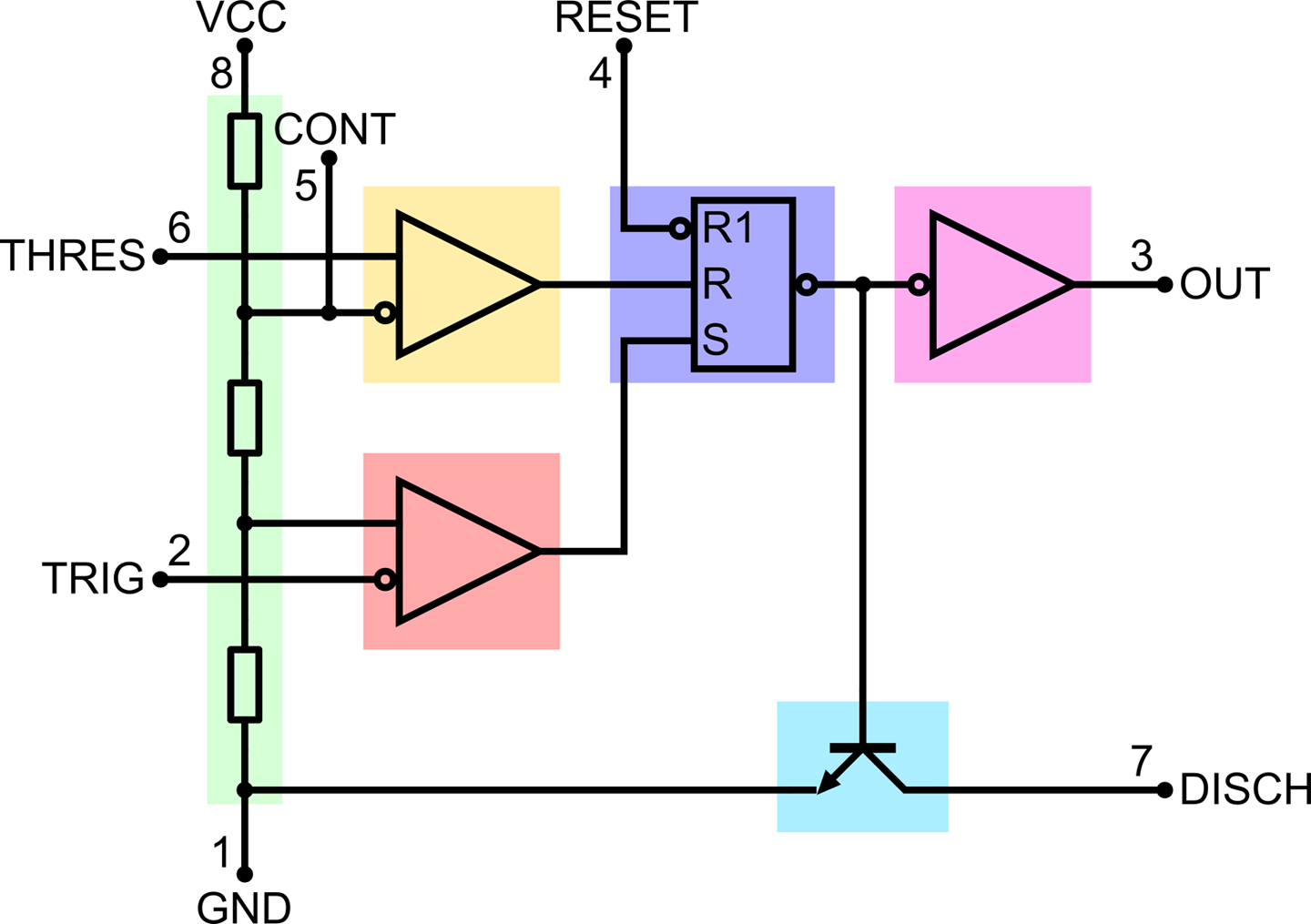
Figure 16-11. A Look Inside an NE555 Timer IC
The design is centered around a reset-set (RS) flip-flop (see Recipe 15.4). This flip-flop has an output that will become high if the S input goes high. It will then stay high until the flip-flop is reset, either by R becoming high or R1 becoming low. The output of the flip-flop drives both a push-pull output stage (Recipe 11.8) connected to the OUT pin and an open-collector output connected to pin DISCH, which is used to discharge a timing capacitor.
Setting and resetting the flip-flop is achieved by using an arrangement of three resistors in a voltage divider from the positive supply (VCC) to GND and two comparitors (Recipe 17.10). If the voltage at TRIG falls below ⅓ of the supply voltage, the lower comparitor sets the flip-flop until the voltage at THRES exceeds ⅔ of the supply voltage and the flip-flop is reset.
The CONT (control) pin is not generally used, but it can be used to adjust the comparitor-threshold voltages. You will also often find schematics where a 10nF capacitor is connected between CONT and GND. This is an additional decoupling capacitor that can improve the oscillator stability, but is by no means essential.
In addition to the standard NE555 timer, a number of variations of the device have been developed. The NE556 is simply a 14-pin IC package that has two NE555 timers in it sharing common supply pins.
The LMC555 is a CMOS version of the 555 timer that is pin compatible and will operate down to 1.5V supply.
See Also
You can find the datasheet for the NE555 here: http://www.ti.com/lit/ds/symlink/ne555.pdf and the datasheet for the 555 here: http://www.ti.com/lit/ds/symlink/lmc555.pdf.
Figure 16-11 is taken from an informative Wikipedia page on the 555 timer: https://en.wikipedia.org/wiki/555_timer_IC.
16.7 Make a One-Shot Timer
Solution
Figure 16-12 shows an NE555 timer configured as a one-shot (monostable) timer.
When SW1 is pressed, OUT becomes HIGH and stays HIGH until either SW2 is pressed (to cancel the timer) or a period of time 1.1 x R1 x C1 has elapsed.
For example, a value of C1 of 100µF and R1 of 100kΩ will give a delay of:
1.1 x 100µ x 100k = 11 seconds
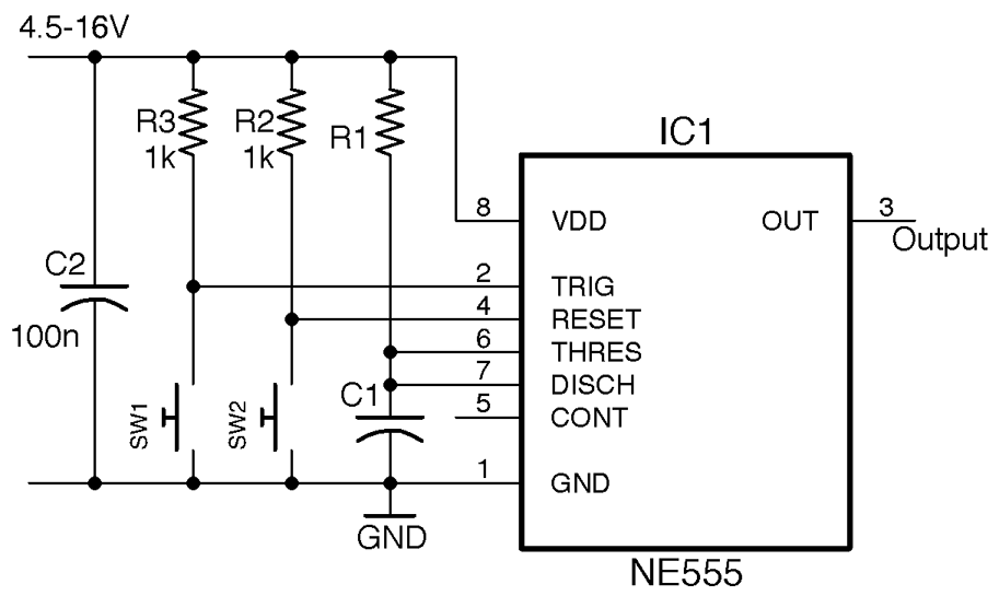
Figure 16-12. Using an NE555 Timer as a One-Shot Timer
Discussion
In this timer circuit to achieve timings of a second or more, you need to use an electrolytic of 100µF or greater.
You can, of course, make R1 a variable resistor, or more likely a fixed resistor and variable resistor in series in order to set a minimum delay.
See Also
For other 555 timer recipes see Recipe 16.5, Recipe 16.6, Recipe 16.8, Recipe 16.9, and Recipe 16.10.
16.8 Control Motor Speed
Solution
Use an NE555 timer as shown in Figure 16-13.
For a PWM frequency of around 1kHz, use a value for R1 of 270Ω, R2 a 10kΩ pot, and C1 100nF.
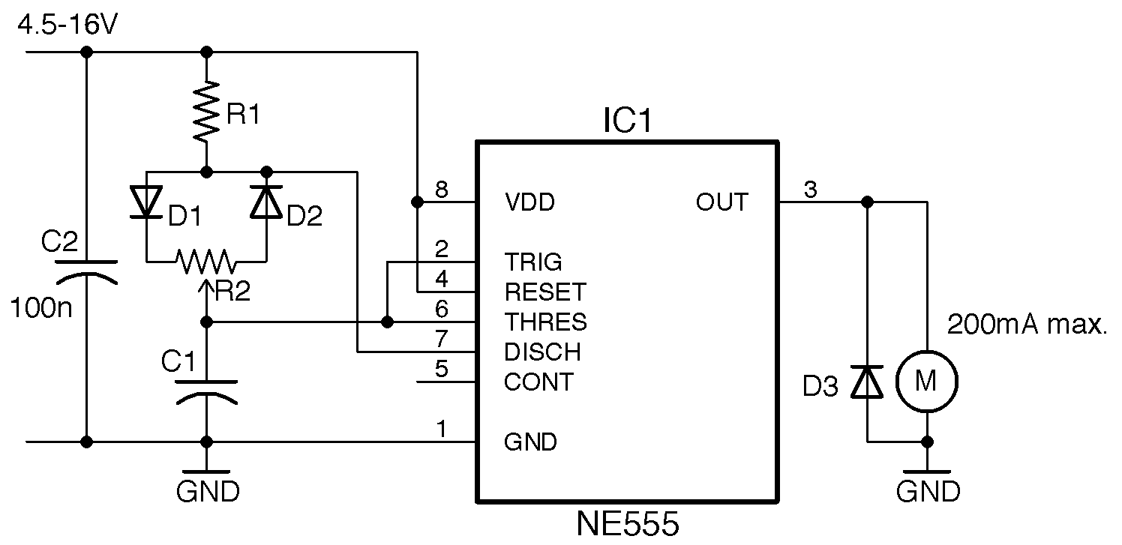
Figure 16-13. PWM Motor Control Using a 555 Timer
Discussion
The NE555 timer output can drive about 200mA, which is only sufficient for a pretty small motor. Drawing more current than this will cause the IC to overheat and eventually fail. To drive a higher power motor, use a transistor as described in Recipe 13.2.
The minimum duty cycle of this circuit depends on the ratio of R1 to R2. R1 should be considerably lower than R2 to minimize the duty cycle, but R1 cannot be 0Ω or the oscillations will stop. A ratio of 40:1 is sufficient to ensure the minimum duty cycle is just 3–4%.
Figure 16-14 shows the minimum duty cycle with the knob of R2 at one end of its travel, Figure 16-15 shows a 50% duty cycle, and Figure 16-16 the maximum duty cycle.
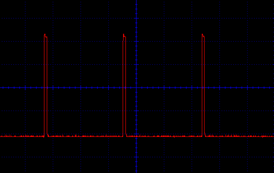
Figure 16-14. PWM Motor Control (Minimum Duty Cycle)
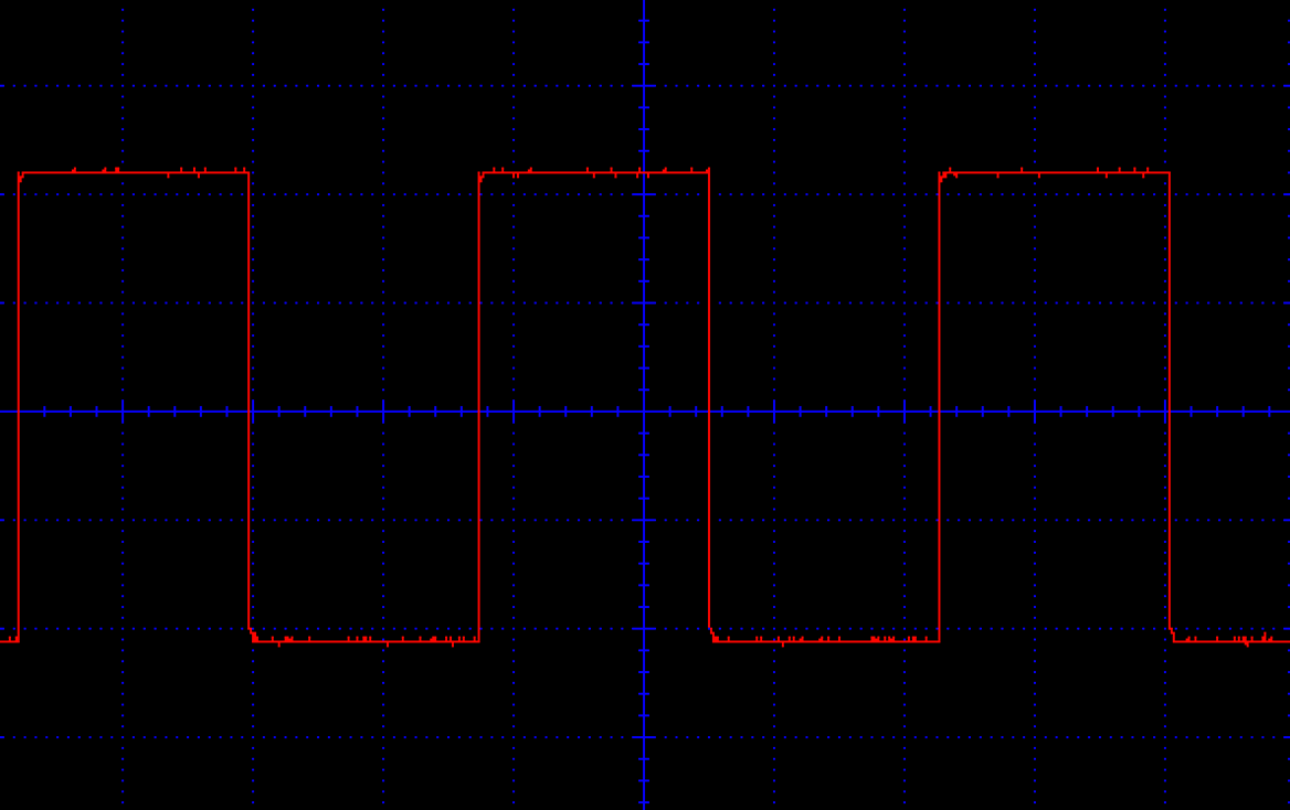
Figure 16-15. PWM Motor Control (50% Duty Cycle)
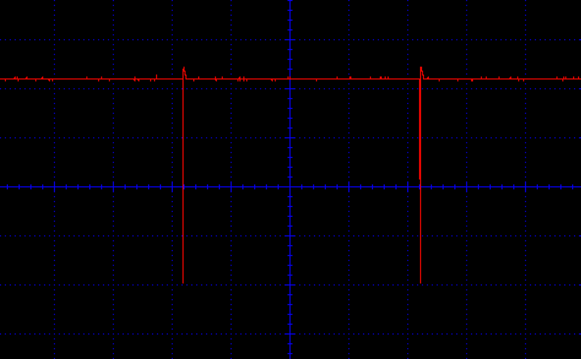
Figure 16-16. PWM Motor Control (Maximum Duty Cycle)
See Also
To use PWM outputs from an Arduino or Raspberry Pi, see Recipe 13.2.
16.9 Apply PWM to an Analog Signal
Solution
Use an NE555 timer in the configuration shown in Figure 16-17.
The analog signal must be between 0 and VCC and is applied to the CONT (control) pin of the IC. The Clock signal should be at the modulation frequency and can be provided by another NE555 timer in a stable configuration as described in Recipe 16.5. Rather than using a separate chip to provide the clock, you can use an NE556, which contains the equivalent of two NE555s in one package.
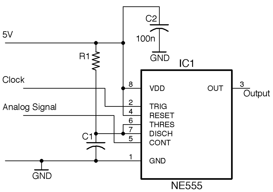
Figure 16-17. PWM of an Analog Signal Using an NE555 Timer
Discussion
The NE555 is configured as a monostable whose pulse length is determined by R1, C1, and the voltage at CONT. This monostable fires every time the TRIG pin pulses in response to the modulation clock.
R1 and C1 set the maximum pulse length, which should be timed to be one wavelength of the clock.
For example, if the clock frequency is 30kHz, the period length is:
1/30k = 33.3µs
The maximum pulse length Tmax (see Recipe 16.7) is:
Tmax = 1.1 R1 C1
So, an R1 of 470Ω and a C1 of 100nF would give a Tmax of:
1.1 × 270 × 100n = 29.7µs
This would allow the full voltage range of 0 to 5V to be modulated as PWM.
The use of two NE555 ICs (or a single NE556) configured as an oscillator providing a clock with the second configured as a monostable is an alternative to Recipe 16.8 for using PWM top-control power to a load. In such a case, the CONT pin could be connected to the slider of a pot connected between 5V and GND to control the pulse width.
See Also
Creating a PWM output signal is the first step in class-D digital amplification (see Recipe 18.5).
To control power to say a motor or other load, see Recipe 16.8.
16.10 Make a Voltage-Controlled Oscillator (VCO)
Solution
Use an NE555 configured as an astable and use the CONT pin voltage to control the switching thresholds and hence the frequency. This arrangement is shown in Figure 16-18.
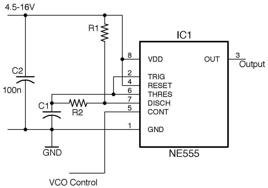
Figure 16-18. Using an NE555 as a VCO
Discussion
VCOs are standard building blocks in analog audio synthesizers, where the output of a low-frequency oscillator can be used to modulate the audio frequency of a VCO.
This VCO design operates over a fairly limited range of frequencies. Using a 5V supply and values of R1 = 1kΩ, R2 = 10kΩ, and C1 = 10nF the plot of Figure 16-19 shows how the frequency varies with the control voltage.
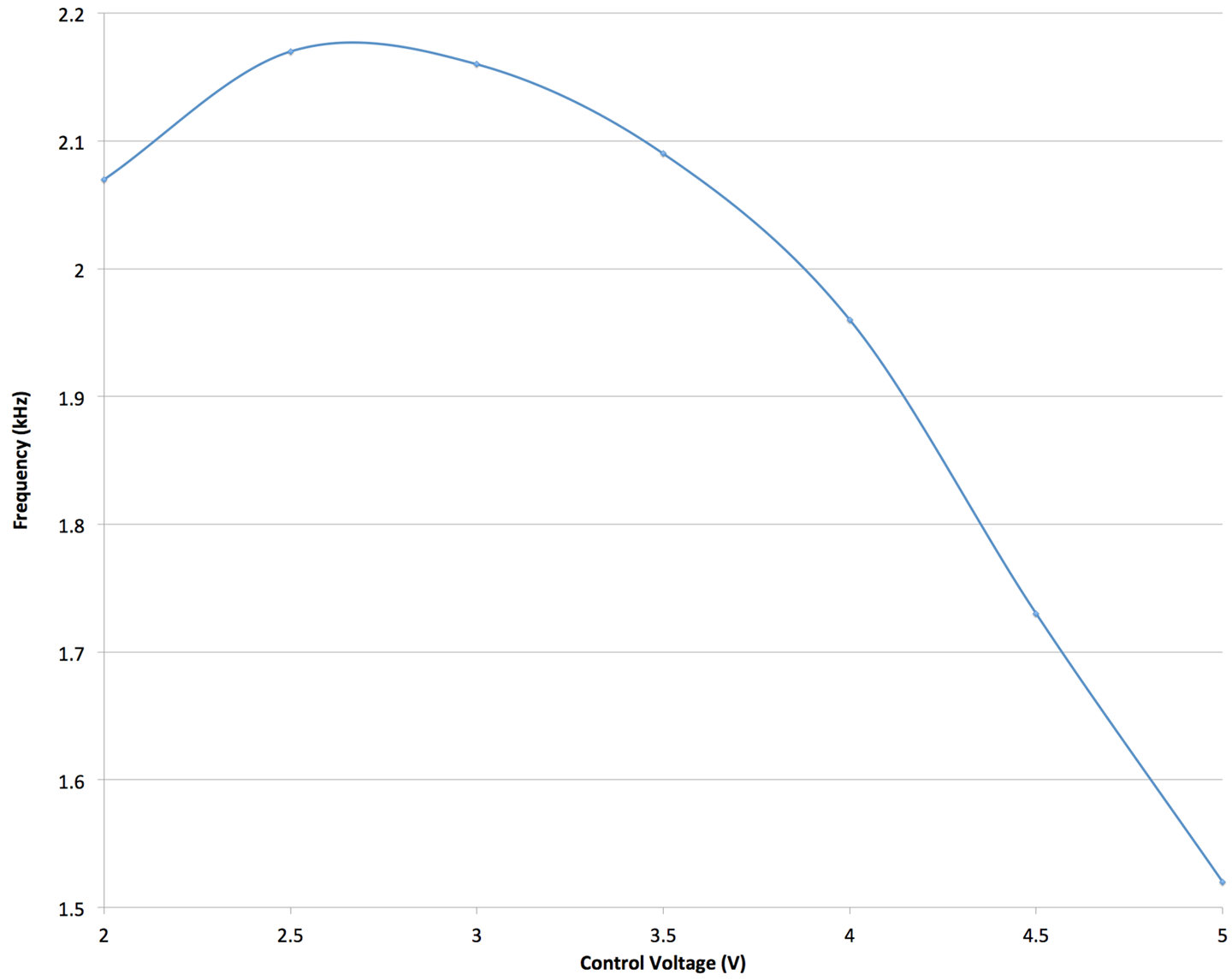
Figure 16-19. Frequency Against Control Voltage
The useful control voltage range is between about 3 and 5V in this example. Oscillation stopped completely below 1.8V.
See Also
For the use of a VCO in an FM transmitter, see Recipe 19.1.
16.11 Explore Decibel Measurement
Solution
The term “decibel” is not strictly speaking a unit of anything, but rather a way of expressing ratios that is suitable for properties such as sound whose perception by humans is logorithmic. That is, for a sound signal to sound a little bit louder, you might need to double the amplitude (voltage).
That is why a 1W amplifier can provide a reasonable volume of sound, but if you need more volume, then rather than take the next step to 2W of output power, you might jump straight to 10W and then on to 100W.
A positive value of dB represents amplification of a signal and a negative dB attenuation (reduction in amplitude) of a signal.
A gain expressed in dB can either apply to voltage (amplitude) or to power, the power being proportional to the amplitude squared. The unit dB is most commonly used with amplitude, in which case the gain is as follows (log is log to the base 10):
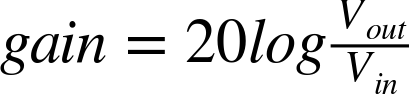
Figure 16-20 shows various common ratios and the dB equivalents.
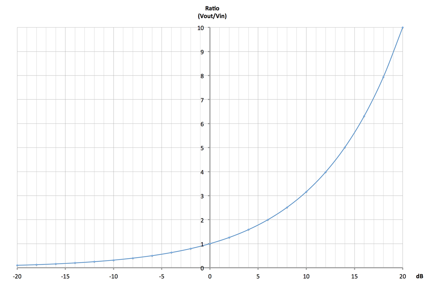
Figure 16-20. Gain and Attenuation of Amplitude Expressed in dB and as a Ratio
A gain of 0dB means the output is exactly the same amplitude as the input. A gain of +6dB means a doubling of the amplitude and –6dB an attenuation of the signal by half.
Table 16-3 shows some common dB ratios and what they mean in terms of amplification or attenuation of both amplitude (voltage) and power.
| dB | Amplitude (Voltage) | Power |
|---|---|---|
| 100 | gain of 100,000 | gain of 10,000,000,000 |
| 80 | gain of 10,000 | gain of 100,000,000 |
| 60 | gain of 1,000 | gain of 1,000,000 |
| 40 | gain of 100 | gain of 10,000 |
| 20 | gain of 10 | gain of 100 |
| 10 | gain of 3.162 | gain of 10 |
| 6 | gain of approx. 2 | gain of 3.981 |
| 3 | gain of 1.413 | gain of approx. 2 |
| 0 | no change | no change |
| –3 | attenuation of 1.413 | attenuation of approx. 2 |
| –6 | attenuation of approx. 2 | attenuation of 3.981 |
| –10 | attenuation of 3.162 | attenuation of 10 |
| –20 | attenuation of 10 | attenuation of 100 |
| –40 | attenuation of 100 | attenuation of 10,000 |
| –60 | attenuation of 1,000 | attenuation of 1,000,000 |
| –80 | attenuation of 10,000 | attenuation of 100,000,000 |
| –100 | attenuation of 100,000 | attenuation of 10,000,000,000 |
See Also
Wikipedia has a useful description of decibels as a unit of gain at http://bit.ly/2lPeant.