Table of Contents for
Electronics Cookbook
 Electronics Cookbook
Published by
O'Reilly Media, Inc., 2017
Electronics Cookbook
Published by
O'Reilly Media, Inc., 2017
- Cover
- nav
- Electronics Cookbook
- Electronics Cookbook
- Preface
- Theory
- Resistors
- Capacitors and Inductors
- Diodes
- Transistors and Integrated Circuits
- Switches and Relays
- Power Supplies
- Batteries
- Solar Power
- Arduino and Raspberry Pi
- Switching
- Sensors
- Motors
- LEDs and Displays
- Digital ICs
- Analog
- Operational Amplifiers
- Audio
- Radio Frequency
- Construction
- Tools
- Parts and Suppliers
- Arduino Pinouts
- Raspberry Pi Pinouts
- Units and Prefixes
- Index
- About the Author
- Colophon
Chapter 5. Transistors and Integrated Circuits
5.0 Introduction
Transistors are used to control the flow of a current. In digital electronics this control takes the form of an on/off action, with the transistor acting as an electronic switch.
Transistors are also used in analog electronics where they can be used to amplify signals in a linear manner. However, these days, a better (cheaper and more reliable) way to do this is to use an integrated circuit (chip) that combines lots of transistors and other components into a single convenient package.
This chapter does not cover all types of transistors or semiconductor devices, but instead focuses on the most common ones, which are generally low in cost and easy to use. There are other exotic devices like the unijunction transistors and SCRs (silicon-controlled rectifiers) that used to be popular, but are now seldom used.
The other thing deliberately left out of this cookbook is the usual theory of how semiconductors like diodes and transistors work. If you are interested in the physics of electronics, there are many books and useful resources on semiconductor theory, but just to make use of transistors, you do not really need to know about holes, electrons, and doping N and P regions.
This chapter will concentrate on the use of transistors in their digital role. You will find information on using transistors for analog circuits in Chapter 16.
In this chapter, you will encounter a wide variety of transistors. Appendix A includes pinouts for the transistors used in this chapter and throughout the book.
5.1 Switch a Stronger Current Using a Weaker One
Solution
Use a low-cost bipolar junction transistor (BJT).
BJTs like the 2N3904 cost just a few cents and are often used with a microcontroller output pin from an Arduino or Raspberry Pi to increase the current the pin can control.
Figure 5-1 shows the schematic symbol for a BJT alongside one of the most popular models of this kind of transistor, the 2N3904. The 2N3904 is in a black plastic package called a TO-92 and you will find that many different low-power transistor models come supplied in the TO-92 package.
The transistor is usually shown with a circle around it, but sometimes just the symbol inside the circle is used.
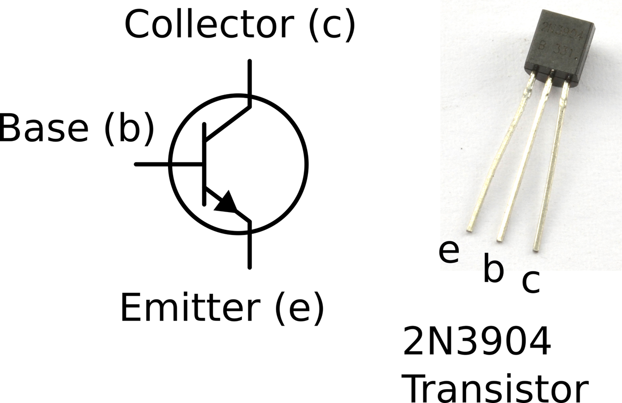
Figure 5-1. A Bipolar Transistor Schematic Symbol and Actual Device
The three connections to the transistor in Figure 5-1 are from top to bottom:
- The collector—the main current to be controlled flows into the collector
- The base—the control connection
- The emitter—the main current flows out through the emitter
The main current flowing into the collector and out of the emitter is controlled by a much smaller current flowing into the base and out of the emitter. The ratio of the base current to the collector current is called the current gain of the transistor and is typically somewhere between 100 and 400. So for a transistor with a gain of 100, a 1mA current flowing from base to emitter will allow a current of up to 100mA to flow from collector to emitter.
Discussion
To get a feel for how such a transistor could be used as a switch, build the circuit shown in Figure 5-2 using the breadboard layout shown in Figure 5-3. For help getting started with breadboard tutorial, see Recipe 20.1.
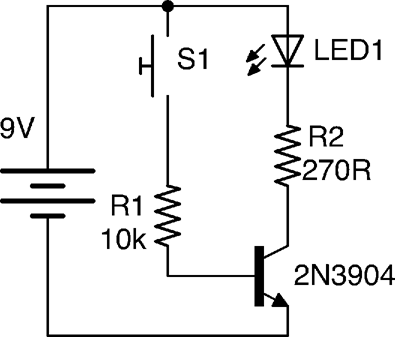
Figure 5-2. A Schematic for Experimenting with a Transistor
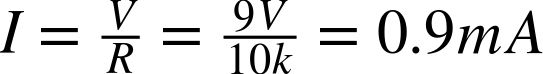
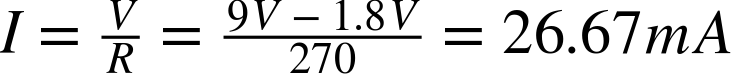
The push switch will turn the LED on when its pressed. Although this could be achieved much more easily by just putting the switch in series with the LED and R2, the important point is that the switch is supplying current to the transistor through R1. A quick calculation shows that the maximum current that could possibly flow through R1 and the base is:
In reality the current is less than this, because we are ignoring the 0.6V between the base and emitter of the transistor. If you want to be more precise, then the current is actually:
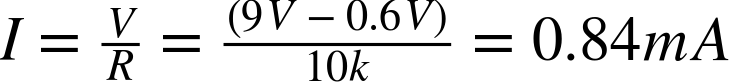
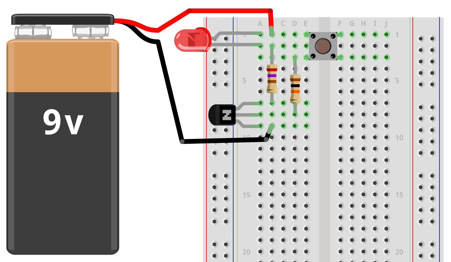
Figure 5-3. A Breadboard Layout for Experimenting with a Transistor
This tiny current flowing through the base is controlling a much bigger current of roughly (assuming Vf of LED 1.8V):
Just like a diode, when the BJT is in use there will be an almost constant voltage drop of around 0.5V to 1V between the base and emitter connections of the transistor.
Limiting Base Current
A resistor limiting the current that can flow into the base of the transistor (R1 in Figure 5-2) is essential, because if too much current flows through the base then the transistor will overheat and eventually die in a puff of smoke.
Because the base of a transistor only requries a small current to control a much bigger current, it is tempting to think of the base as having a built-in resistance to a large current flowing. This is not the case, since it will draw a self-destructively large current as soon as its base voltage exceeds 0.6V or so. So, always use a base resistor like R1.
The BJT transistor described earlier is the most common and is an NPN type of transistor (negative positive negative). This is not a case of the transistor being indecisive, but relates to the fact that the transistor is made up like a sandwich with N-type (negative) semiconductor as the bread and P-type (positive) semiconductor as the filling. If you want to know what this means and understand the physics of semiconductors, then take a look at https://en.wikipedia.org/wiki/Bipolar_junction_transistor.
There is another less commonly used type of BJT called a PNP (positive negative positive) transistor. The filling in this semiconductor sandwich is negatively doped. This means that everything is flipped around. In Figure 5-2 the load (LED and resistor) is connected to the positive end of the power supply and switched on the negative side to ground. If you were to use a PNP transistor the circuit would look like Figure 5-4. You can find out more about using PNP transistors in Recipe 11.2.
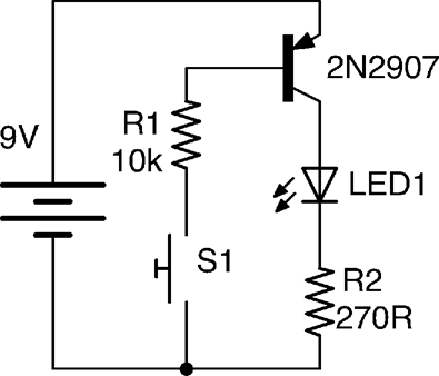
Figure 5-4. Using a PNP Transistor
See Also
If the gain of your transistor is not enough, you may need to consider a Darlington transistor (Recipe 5.2) or MOSFET (Recipe 5.3).
If, on the other hand, you need to switch a high-power load then you should consider a power MOSFET (Recipe 5.3) or IGBT (Recipe 5.4).
You can find the datasheet for the popular low-power BJT, the 2N3904, here: http://www.farnell.com/datasheets/1686115.pdf.
5.2 Switch a Current with Minimal Control Current
Solution
Use a Darlington transistor.
A regular BJT will typically only have a gain (ratio of base current to collector current) of perhaps 100. A lot of the time, this will be sufficient, but sometimes more gain is required. A convenient way of achieving this is to use a Darlington transistor, which will typically have a gain of 10,000 or more.
A Darlington transistor is actually made up of two regular BJTs in one package as shown in Figure 5-5. Two common Darlington transistors are shown next to the schematic symbol. The smaller one is the MPSA14 and the larger the TIP120. See Recipe 5.5 for more information on these transistors.
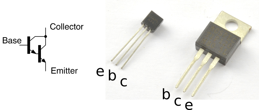
Figure 5-5. Darlington Transistors
The overall current gain of the pair of transistors in this arrangement is the gain of the first transistor multiplied by the gain of the second. It’s easy to see why this is the case, as the base of the second transistor is supplied with current from the collector of the first.
Discussion
Although you can use a Darlington transistor in designs just as if it were a single BJT, one effect of arranging the transistors like this is that there are now two voltage drops between the base and emitter. The Darlington transistor behaves like a regular NPN BJT with an exceptionally high gain but a base-emitter voltage drop of twice that of a normal BJT.
A popular and useful Darlington transistor is the TIP120. This is a high-power device that can handle a collector current of up to 5A.
See Also
You can find the datasheet for the TIP120 here: http://bit.ly/2mHBQy6 and the MPSA14 here: http://bit.ly/2mI1vXF.
5.3 Switch High Current Loads Efficiently
Solution
MOSFETs (metal-oxide semiconductor field effect transistors) do not have an emitter, base, and collector, but rather a source, gate, and drain. Like BJTs, MOSFETs come in two flavors: N-channel and P-channel. It is the N-channel that is most used and will be described in this recipe. Figure 5-6 shows the schematic symbol for an N-channel MOSFET with a couple of common MOSFETs next to it. The larger transistor (in a package called TO-220) is an FQP30N06 transistor capable of switching 30A at 60V. The hole in the TO-220 package is used to bolt it to a heatsink, something that is only necessary when switching high currents. The small transistor on the right is the 2N7000, which is good for 500mA at 60V.
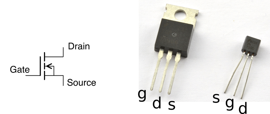
Figure 5-6. MOSFETs
Rather than multiply a current in the way that a BJT does, there is no electrical connection between the gate and other connections of the MOSFET. The gate is separated from the other connections by an insulating layer. If the gate-drain voltage exceeds the threshold voltage of the MOSFET, then the MOSFET conducts and a large current can flow between the drain and source connections of the MOSFET. The threshold voltage varies between 2V and 10V. MOSFETs designed to work with digital outputs from a microcontroller such as an Arduino or Raspberry Pi are called logic-level MOSFETs and have a gate-threshold voltage guaranteed to be below 3V.
If you look at the datasheet for a MOSFET you will see that it specifies on and off resistances for the transistor. An on resistance might be as low as a few mΩ and the off resistance many MΩ. This means that MOSFETs can switch much higher currents than BJTs before they start to get hot.
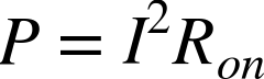
You can calculate the heat power generated by the MOSFET using the current flowing through it and its on resistance using the following formula. For more information on power, see Recipe 1.6.
Discussion
The schematic and breadboard layout used in Recipe 5.1 needs a little modification to be used to experiment with a MOSFET. The variable resistor is now used to set the gate voltage from 0V to the battery voltage. The revised schematic and breadboard layouts are shown in Figures 5-7 and 5-8, respectively.
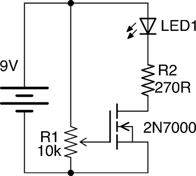
Figure 5-7. Schematic for Experimenting with a MOSFET
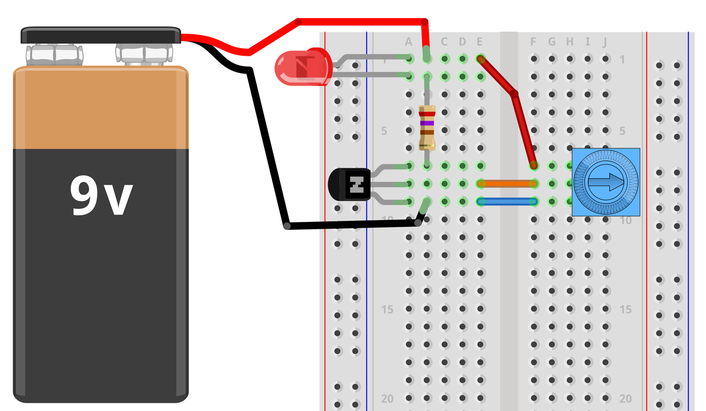
Figure 5-8. Breadboard Layout for Experimenting with a MOSFET
With the trimpot’s knob at the 0V end of its track, the LED will not be lit. As the gate voltage increases to about 2V the LED will start to light and when the gate voltage gets to about 2.5V the LED should be fully on.
Try disconnecting the end of the lead going to the slider of the pot and touch it to the positive supply from the battery. This should turn the LED on, and it should stay on even after you take the lead from the gate away from the positive supply. This is because there is sufficient charge sitting on the gate of the MOSFET to keep its gate voltage above the threshold. As soon as you touch the gate to ground, the charge will be conducted away to ground and the LED will extinguish.
Since MOSFETs are voltage- rather than current-controlled devices you might be surprised to find that under some circumstances you do have to consider the current flowing into the gate. That is because the gate acts like one terminal of a capacitor. This capacitor has to charge and discharge and so when pulsed at high frequency the gate current can become significant. Using a current-limiting resistor to the gate will prevent too much current from flowing.
Another difference between using a MOSFET and a BJT is that if the gate connection is left floating, then the MOSFET can turn on when you aren’t expecting it. This can be prevented by connecting a resistor between the gate and source of the MOSFET.
See Also
To use MOSFETs with a microcontroller output, see Recipe 11.3.
To use a MOSFET for polarity protection, see Recipe 7.17.
For level shifting using a MOSFET, see Recipe 10.17.
For the use of heatsinks, see Recipe 20.7.
5.4 Switch Very High Voltages
Solution
An IGBT (insulated gate bipolar transistor) is an exotic type of transistor found in high-power, high-voltage switching applications. They are fast switching, and generally are particularly well specified when it come to operating voltage. Switching voltages of 1000V are not uncommon.
A BJT has base, emitter, and collector; a MOSFET has a gate, source, and drain; and an IGBT combines the two, having a gate, emitter, and collector. Figure 5-9 shows the schematic symbol for an IGBT alongside two IGBTs. The smaller of the two (STGF3NC120HD) is capable of switching 7A at 1.2kV and the even bigger one (IRG4PC30UPBF) 23A at 600V.
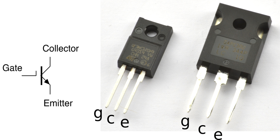
Figure 5-9. The Schematic Symbol for an IGBT and Two IGBTs
Discussion
IGBTs are voltage-controlled devices just like a MOSFET, but the switching side of the transistor behaves just like a BJT. The gate of an IGBT will have a threshold voltage just like a MOSFET.
IGBTs are sometimes used in the same role as high-power MOSFETs but have the advantage over MOSFETs of being able to switch higher voltages at equally large currents.
See Also
For information on BJTs see Recipe 5.1 and for MOSFETS see Recipe 5.3.
You can find the datasheet for the STGF3NC120HD here: http://bit.ly/2msNM6v.
The IRG4PC30UPBF datasheet is here: http://bit.ly/2msXTb9.
5.5 Choosing the Right Transistor
Solution
Stick to a basic set of go-to transistors for most applications until you have more unusual requirements and then find something that fits the bill.
A good set of go-to transistors is shown in Table 5-1.
| Transistor | Type | Package | Max. Current | Max. Volts |
|---|---|---|---|---|
| 2N3904 | Bipolar | TO-92 | 200mA | 40V |
| 2N7000 | MOSFET | TO-92 | 200mA | 60V |
| MPSA14 | Darlington | TO-92 | 500mA | 30V |
| TIP120 | Darlington | TO-220 | 5A | 60V |
| FQP30N06L | MOSFET | TO-220 | 30A | 60V |
When shopping for an FQP30N06L, make sure the MOSFET is the “L” (for logic) version, with “L” on the end of the part name; otherwise, the gate-threshold voltage requirement may be too high to connect the gate of the transistor to a microcontroller output especially if it is operating at 3.3V.
The MPSA14 is actually a pretty universally useful device for currents up to 1A, although at that current there is a voltage drop of nearly 3V and the device gets up to a temperature of 120°C! At 500mA, the voltage drop is a more reasonable 1.8V and the temperature 60°C.
To summarize, if you only need to switch around 100mA then a 2N3904 will work just fine. If you need up to 500mA, use an MPSA14. Above that, the FQP30N06L is probably the best choice, unless price is a consideration, because the TIP120 is considerably cheaper.
Discussion
Reasons for straying from the transistors listed in Table 5-1 include:
- You need to switch at high frequency—look for BJTs or FETs described as RF.
- You need to switch higher voltages—BJTs and MOSFETs are readily available at quite high voltages up to 400V, but for even higher voltages look at IGBTs.
- For high currents, MOSFETs take a beating. Look for devices with the lowest possible resistance as this will be the main thing that determines how hot it gets and therefore how much current it can cope with before it fails.
See Also
For information on BJTs see Recipe 5.1, for MOSFETs Recipe 5.3, and for IGBTs Recipe 5.4.
To decide on a transistor for switching with an Arduino or Raspberry Pi, see Recipe 11.5.
Once you start to push transistors beyond a light load, you will find that they start to get hot. If they get too hot they will burn out and be permanently destroyed. To avoid this, either use a transistor with greater current-handling capability or fix a heatsink to it (Recipe 20.7).
5.6 Switching Alternating Current
Solution
TRIAC (TRIode for alternating current) is a semiconductor-switching device designed specifically to switch AC.
BJT and MOSFETs are not useful for switching AC. They can only do that if you split the positive and negative halves of the cycle and switch each with a separate transistor. It is far better to use a TRIAC that can be thought of as a switchable pair of back-to-back diodes.
Figure 5-10 shows how a TRIAC might be used to switch a high AC load using a small current switch. A circuit like this is often used so that a small low-power mechanical switch can be used to switch a large AC current.
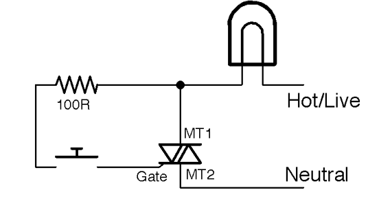
Figure 5-10. Switching AC with a TRIAC
Switching High-Voltage AC
The 110V or 220V AC that you find in your home kills thousands of people every year. It can burn you and it can stop your heart, so please do not attempt to build the circuits described here unless you are absolutely sure that you can do so safely.
Also, see Recipe 21.12.
Discussion
When the switch is pressed a small current (tens of milliamps) flows into the gate of the TRIAC. The TRIAC conducts and will continue conducting until the AC crosses zero volts again. This has the benefit that the power is switched off at low power when the voltage is close to zero, reducing the power surges and electrical noise that would otherwise occur if switching inductive loads like motors.
However, the load could still be switched on at any point in the circuit, generating considerable noise. Zero-crossing circuits (see Recipe 5.9) are used to wait until the next zero crossing of the AC before turning the load on, reducing electrical noise further.
See Also
See Recipe 1.7 on AC.
For information on solid-state relays using TRIACs, see Recipe 11.10.
TRIACs are usually supplied in TO-220 packages. For pinouts, see Appendix A.
5.7 Detecting Light with Transistors
Solution
A phototransistor is essentially a regular BJT with a translucent top surface that allows light to reach the actual silicon of the transistor. Figure 5-11 shows how you can use a phototransistor to produce an output voltage that varies as the level of light falling on the transistor changes.
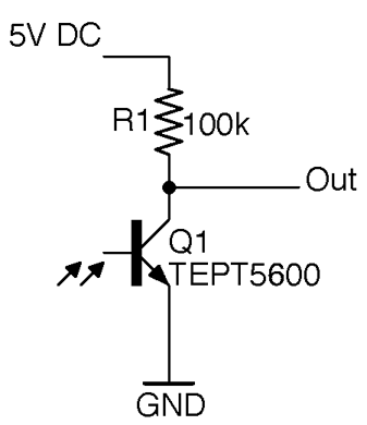
Figure 5-11. Using a Phototransistor
When the photoresistor is brightly illuminated, it will turn on and conduct, pulling the output voltage toward 0V. In complete darkness, the transistor will be completely off and the output voltage will rise to the supply voltage of 5V.
Discussion
Some phototransistors look like regular transistors with three pins and a clear top and others (like the TEPT5600 used in Figure 5-11) come in LED-like packages with pins for the emitter and collector, but no pin for the base. For phototransistors that look like LEDs, the longer pin is usually the emitter. Phototransistors are nearly always NPN devices.
As a light-sensing element, the phototransistor is more sensitive than a photodiode and responds more quickly than a photoresistor. Phototransistors have the advantage over photoresistors that they are manufactured using cadmium sulphide and some countries have trade restrictions on devices containing this material.
See Also
The output of the circuit of Figure 5-11 can be directly connected to an Arduino’s analog input (Recipe 10.12) to take light readings as an alternative to using a photoresistor (Recipe 12.3 and Recipe 12.6).
For the TEPT5600 datasheet, see http://bit.ly/2m8vhS0.
5.8 Isolating Signals for Safety or Noise Elimination
Solution
Use an opto-coupler, which consists of an LED and phototransistor sealed in a single lightproof package.
Figure 5-12 shows how an opto-coupler can be used. When a voltage is applied across the + and – terminals, a current flows through the LED and it lights, illuminating the phototransistor and turning on the transistor. This brings the output down to close to 0V. When the LED is not powered, the transistor is off and R1 pulls the output up to 5V.
The important point is that the lefthand side of the circuit has no electrical connection to the righthand side. The link is purely optical.
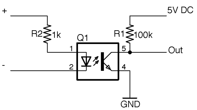
Figure 5-12. An Opto-Coupler
Discussion
When the sensing transistor is a TRIAC (see Recipe 5.6) the device is known as an opto-isolator rather than opto-coupler and the low-power TRIAC inside the opto-isolator can be used to switch AC using a more powerful TRIAC as shown in Figure 5-13. This circuit is often called an SSR (solid-state relay) as it performs much the same role as a relay would in AC switching, but without the need for any moving parts.
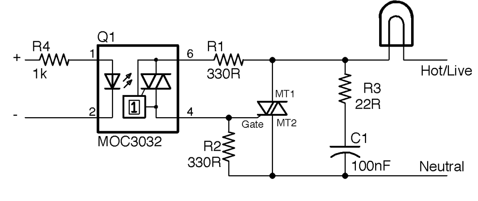
Figure 5-13. An SSR Design
Switching AC Is Dangerous
You should not work with high voltages unless you are completely sure that you can do so safely and understand the risks. See Recipe 21.12 for more information on working with high voltages.
R1 is used to limit the current flowing into the gate of the opto-isolator and R2 keeps the TRIAC MT1 turned off until the TRIAC in the opto-isolator is turned on by light falling on it because of the LED being energized. R3 and C1 form a filter to reduce the RF noise that would otherwise be generated by the switching. Note that R3 and C1 must both be rated to cope with the peak AC voltage (use 400V devices).
The MOC3032 package also contains a zero-crossing switch that stops the TRIAC from turning on until the AC crosses 0V. This greatly reduces the interference generated by the switching circuit.
See Also
For SSRs use opto-isolators, see Recipe 11.10.
For the MOS3032 datasheet, see http://www.farnell.com/datasheets/2151740.pdf.
For relays that also isolate the control side from the power side, see Recipe 6.4.
5.9 Discover Integrated Circuits
Solution
ICs will be involved in almost every project you are likely to work on. Be it a microcontroller or special-purpose chip for motor control or a radio receiver or audio amplifier, there is probably a chip for it. There is little point in building a circuit out of transistors and other components if there is a single IC that will do the job. You will find many different sorts of IC scattered throughout this book.
ICs come in many different shapes and sizes. Figure 5-14 shows a selection of them.
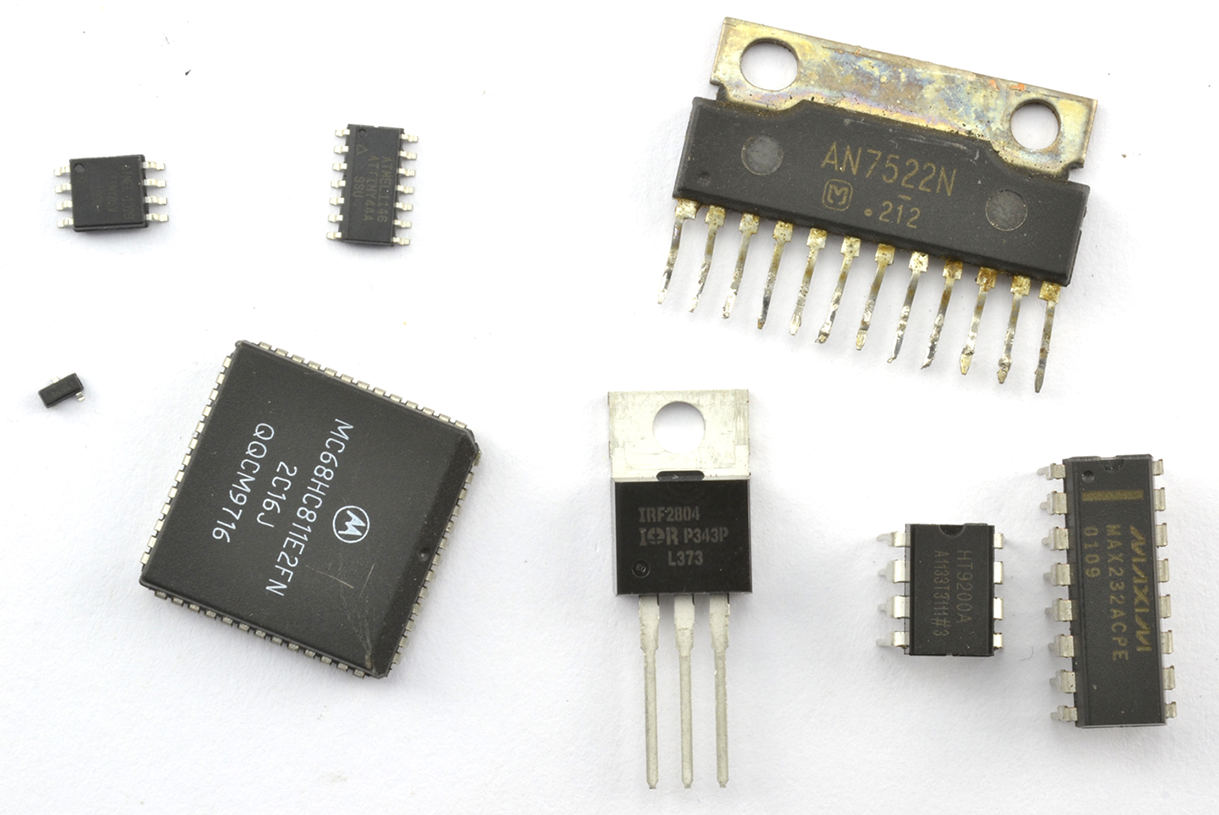
Figure 5-14. A Selection of ICs
Discussion
ICs can have as few as three pins or hundreds of pins. You will often find that the same basic IC is available in different packages, both SMD and through-hole packages. This can be very useful if you plan to prototype your design using a solderless breadboard before manufacturing using SMD components.
Another way of using SMDs on a solderless breadboard is to use a “breakout board” that allows you to solder the SMD onto a board and then plug that board into the breadboard. There is an example of this shown in Figure 18-5.
ICs are identified by their part number, which is often difficult to read, so it’s a good idea to label the bag the IC comes in.
ICs with more than three pins will have a little dot next to pin 1. If there is no dot, then there will be a notch that indicates the top of the IC. The pin numbering then moves down the IC to the bottom continuing with the bottom pin of the righthand side. For some example IC pinouts, see Appendix A.
See Also
You can find a list of the ICs used in this book in “Integrated Circuits”.