Table of Contents for
ARM Assembly Language, 2nd Edition
 ARM Assembly Language, 2nd Edition
Published by
Chapman and Hall/CRC, 2016
ARM Assembly Language, 2nd Edition
Published by
Chapman and Hall/CRC, 2016
- Contents
- ARM Assembly Language: Fundamentals and Techniques, Second Edition
- Preliminaries
- To our families
- Preface
- Acknowledgments
- Authors
- Chapter 1 - An Overview of Computing Systems
- Chapter 2 - The Programmer’s Model
- Chapter 3 - Introduction to Instruction Sets: v4T and v7-M
- Chapter 4 - Assembler Rules and Directives
- Chapter 5 - Loads, Stores, and Addressing
- Chapter 6 - Constants and Literal Pools
- Chapter 7 - Integer Logic and Arithmetic
- Chapter 8 - Branches and Loops
- Chapter 9 - Introduction to Floating-Point: Basics, Data Types, and Data Transfer
- Chapter 10 - Introduction to Floating-Point: Rounding and Exceptions
- Chapter 11 - Floating-Point Data-Processing Instructions
- Chapter 12 - Tables
- Chapter 13 - Subroutines and Stacks
- Chapter 14 - Exception Handling: ARM7TDMI
- Chapter 15 - Exception Handling: v7-M
- Chapter 16 - Memory-Mapped Peripherals
- Chapter 17 - ARM, Thumb and Thumb-2 Instructions
- Chapter 18 - Mixing C and Assembly
- Appendix A: Running Code Composer Studio
- Appendix B: Running Keil Tools
- Appendix C: ASCII Character Codes
- Appendix D
- Glossary
- References
Chapter 16
Memory-Mapped Peripherals
16.1 Introduction
Modern embedded systems generally demand quite a bit from a single piece of silicon. For example, in the 1990s, cell phones were used for making phone calls and little else. Today, their uses range from checking e-mail to watching your favorite movie. The industry also geared up to include GPS on smartphones, so that when you miss that turn while driving down the road (probably because you were arguing with your smartphone), you can also ask it for directions. To build such systems, the hardware has to include more features in silicon, and the software has to learn to talk to those new features. SoC designs are packing ever more devices onto one die. Even off-the-shelf microcontrollers are getting more elaborate, with small, 32-bit processors built to control different types of serial interfaces, e.g., UARTs, I2C, and CAN; analog devices like temperature sensors and analog comparitors; and motion controllers for motors and servos. How are all of these attached to a single processor? In this chapter, we’re going to look at three particular microcontrollers, the LPC2104 and the LPC2132 from NXP, and the TM4C123GH6PM from TI, along with three very useful peripherals, the UART, general-purpose I/O (GPIO), and the digital-to-analog converter (DAC). The UART is a relatively simple serial interface, and we’ll program it to send character data to a window in the simulator. The DAC takes a 10-bit value and generates an output relative to a reference voltage. To show off our coding skills, the DAC will generate a sine wave from the sine table we created in Chapter 12. The last example uses an inexpensive evaluation module, the Tiva Launchpad, to continuously change the color of a flashing LED. In writing the three programs, we’re going to tie all of the elements from previous chapters into the code, including
- Subroutines and how they are written
- Passing parameters
- The ARM Application Procedure Call Standard (AAPCS)
- Stacks
- Q notation
- Arithmetic
- The ARM and Thumb-2 instruction sets
16.2 The LPC2104
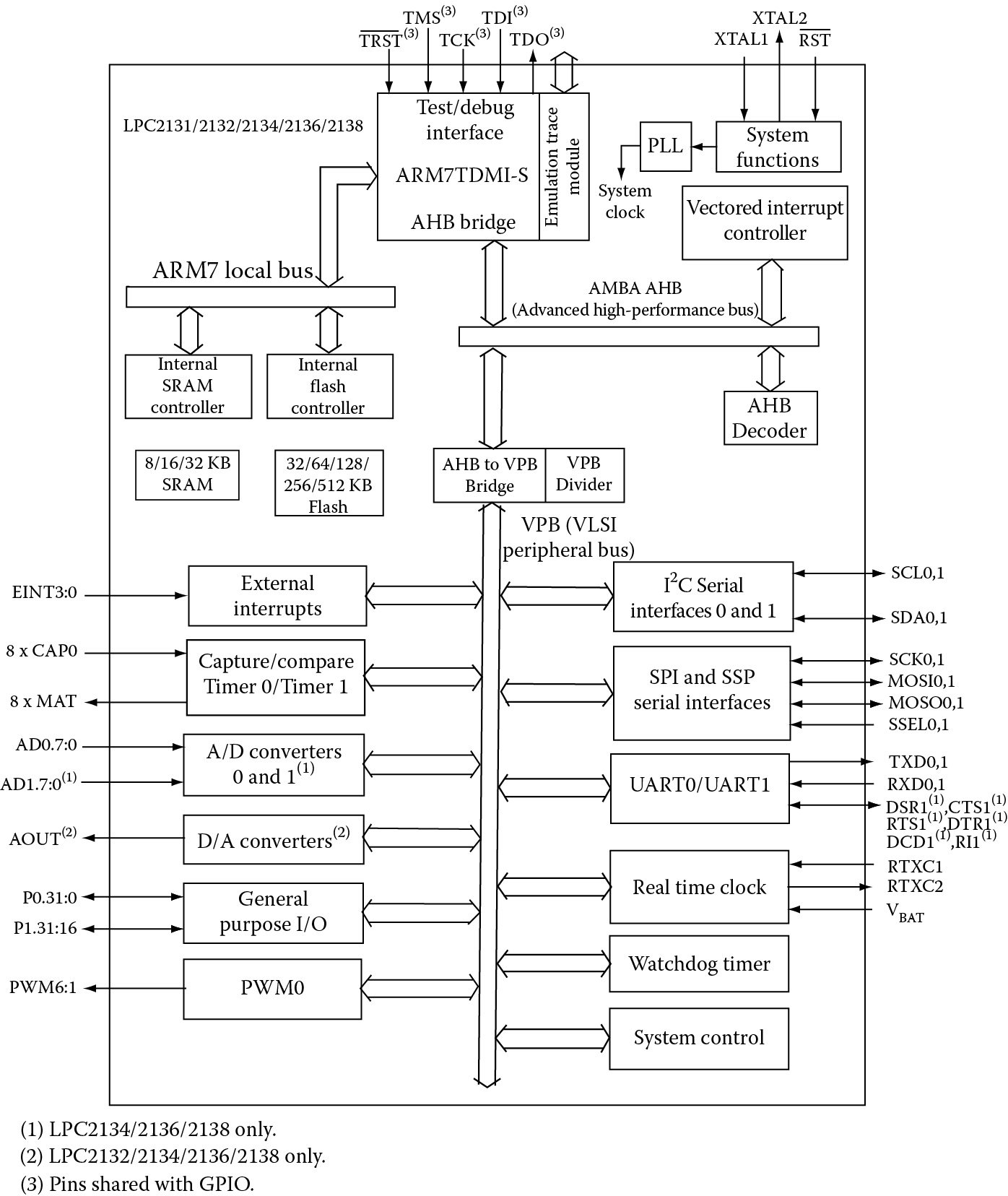
The best place to start is at the highest level—the SoC, or in our case, the microcontroller. Figure 16.1 shows the block diagram of the LPC2104 from NXP. You can see the ARM7TDMI core at the top, and two main busses in the system: the AHB, a high-speed bus designed to have only a few bus masters attached to it, and the VPB, a slower bus designed to have many peripherals attached to it. Between the two busses is a bridge. Fortunately for the programmer, you don’t have to focus too much on the internal hardware design, but it is important to know how the peripherals are attached and what type of interface they have (i.e., what pins go with which peripheral). The LPC2104 includes a few different serial interfaces, along with some timers, some general-purpose I/O, two UARTs, and some on-chip memory. Specifically, we’re going to use UART0 to write some character data out of the part.
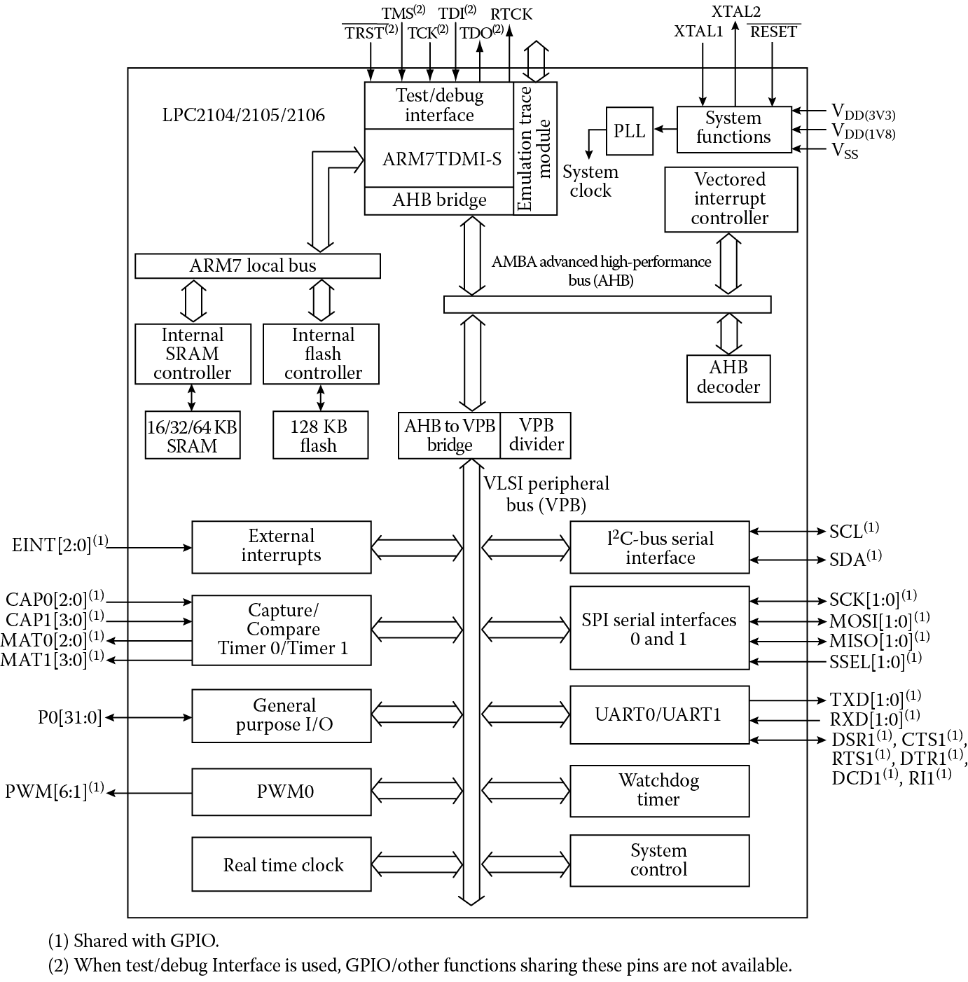
LPC2104/2105/2106 block diagram. (From Doc. LPC2104–2105–2106–6 Product Data Sheet, NXP Semiconductors, July 2007. With permission.)
16.2.1 The UART
The Universal Asynchronous Receiver/Transmitter (UART) is probably one of the most ubiquitous peripherals found on microcontrollers. It can be used to implement serial transmission standards such as RS-232 or EIA232F, or connect the microcontroller to devices like LCD displays or bar code scanners. While high-speed serial standards such as USB and Firewire have largely replaced the older protocols, UARTs are still used to provide a simple, inexpensive interface to devices that don’t necessarily have to transmit and receive data at high speeds.
Asynchronous start-stop communication is done without a clock signal. Rather than using a dedicated clock line, which adds pins, special bits are added to the data being sent to tell the receiver when the data is starting and stopping. Parity bits, like those discussed in Chapter 7, can be added to the transmission. Long ago, these options were all controlled by hardware, through either switches or jumpers. With modern systems, software controls these choices. Table 16.1 shows the options available for character length, stop bits, parity, and break control. You can find more detailed information on UARTs and asynchronous serial ports in (Clements 2000) and (Kane et al. 1981).
UART Configuration Bits in the Control Register
|
U0LCR |
Function |
Description |
Reset Value |
|
1:0 |
Word Length Select |
00:5-bit character length |
0 |
|
01:6-bit character length |
|||
|
10:7-bit character length |
|||
|
11:8-bit character length |
|||
|
2 |
Stop Bit Select |
0:1 stop bit |
0 |
|
1:2 stop bits (1.5 if U0LCR[1:0] = 00) |
|||
|
3 |
Parity Enable |
0: Disable parity generation and checking |
0 |
|
1: Enable parity generation and checking |
|||
|
5:4 |
Parity select |
00: Odd parity |
0 |
|
01: Even parity |
|||
|
10: Forced “l” stick parity |
|||
|
11: Forced “0” stick parity |
|||
|
6 |
Break Control |
0: Disable break transmission |
0 |
|
1: Enable break transmission. Output pin UART0 TxD is forced to logic 0 when U0LCR6 is actively high |
|||
|
7 |
Divisor Latch |
0: Disable access to divisor latches |
0 |
|
Access Bit |
1: Enable access to divisor latches |
16.2.2 The Memory Map
Peripherals on the LPC2104 are memory-mapped, meaning that their configuration registers, receive and transmit buffers, status registers, etc., are each mapped to an address. Accessing peripherals is actually just as easy as accessing a memory block. You can use LDR and STR instructions just as you would if you were writing a value to memory; although, you should be aware that some peripherals are sensitive to reads and writes. For example, a memory-mapped register may automatically clear its contents after being read.
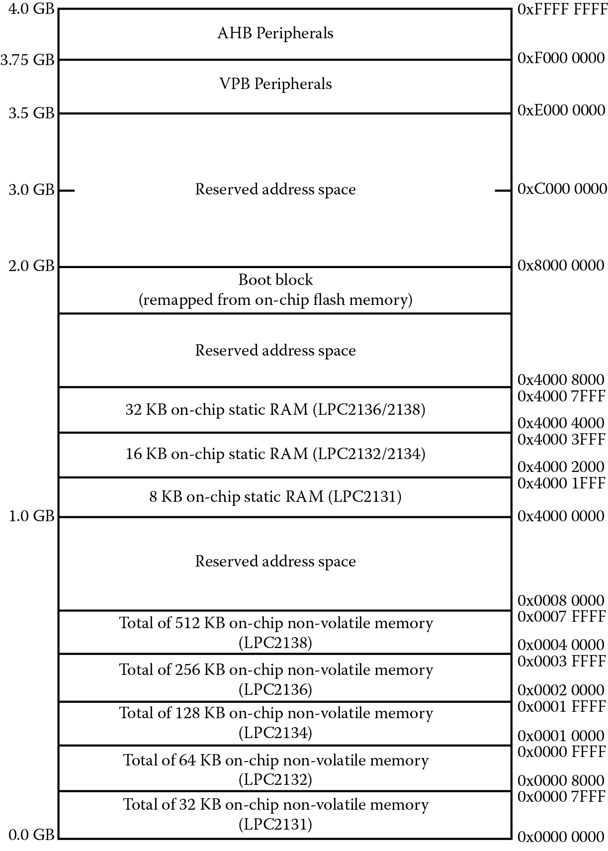
Looking at Figure 16.2, you can see the memory map for the entire microcontroller. Notice that distinct memory regions are defined. The controller comes with 128 KB of Flash memory for your programs, and in the case of the LPC2104, 16 KB of on-chip RAM for building stacks and holding variables. All of the peripherals lie in the very highest addresses, between addresses 0xE0000000 and 0xFFFFFFFF. If we zoom in a bit more, we will find our UART, called UART0, between addresses 0xE000C000 and 0xE000C01C, as shown in Figure 16.3.
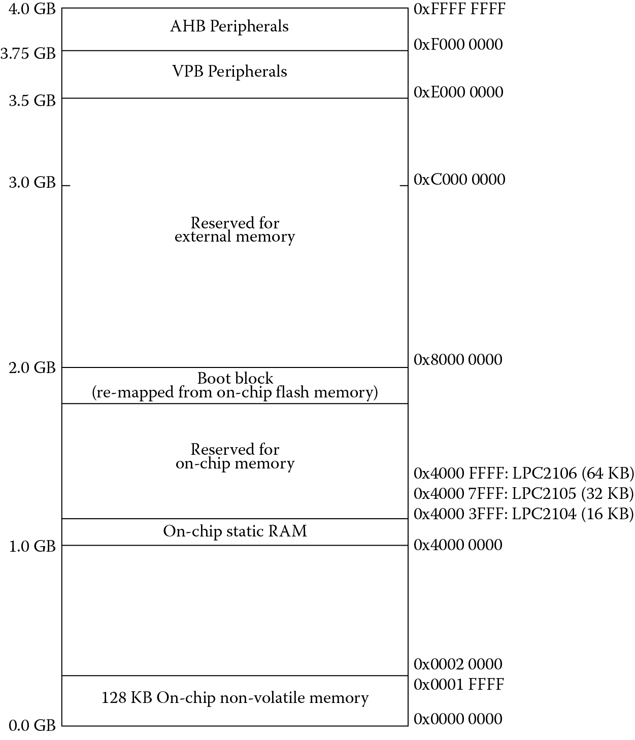
System memory map. (From LPC2106/2105/2104 User Manual NXP Semiconductors, September 2003. With permission.)
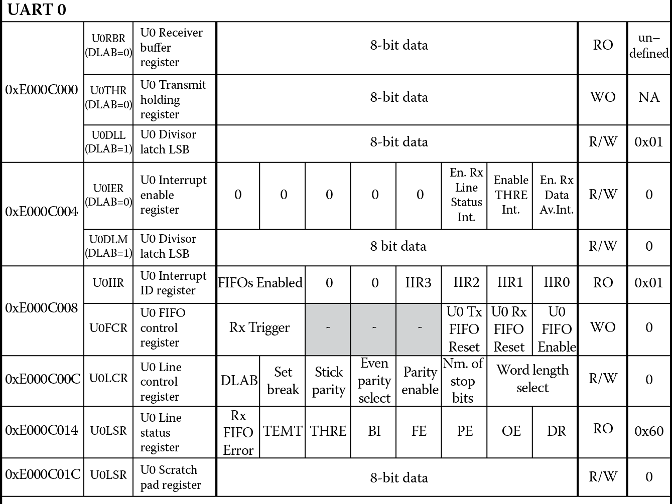
Memory map of UART0 on the LPC2104. (From LPC2106/2105/2104 User Manual NXP Semiconductors, September 2003. With permission.)
16.2.3 Configuring the UART
To demonstrate how easy it is to talk to a peripheral, we’ll write a short block of code that does two things: it calls a subroutine to configure our UART, and it then sends a short message through the UART for the Keil tools to read. If you look at the external pins of the LPC2104, shown in Figure 16.4, you will notice that they are multiplexed pins, meaning that the function of the pin itself is configurable. This allows a package to reduce the pin count, but the programmer must configure the pins to use them. So the first order of business is to set up the LPC2104 so that pins P0.0 and P0.1 become our transmit and receive pins, Tx0 and Rx0, respectively. To do this, we load the address of the pin configuration register, shown in Table 16.2, into a general register, where PINSEL0 is equated to 0xE002C000. Using a read-modify-write sequence (good practice when you don’t want to disturb other configuration or status bits), PINSEL0[1:0] and PINSEL0[3:2] are set to 0b01. The assembly would look like the following:
PINSEL0 Register for Pin Configurations
|
PINSEL0 |
Pin Name |
Function When 00 |
Function When 01 |
Function When 10 |
Function When 11 |
Reset Value |
|
1:0 |
P0.0 |
GPIO Port 0.0 |
TxD (UART 0) |
PWM1 |
Reserved |
0 |
|
3:2 |
P0.1 |
GPIO Port 0.1 |
RxD (UART 0) |
PWM3 |
Reserved |
0 |
|
5:4 |
P0.2 |
GPIO Port 0.2 |
SCL (l2 C) |
Capture 0.0 (Timer 0) |
Reserved |
0 |
|
7:6 |
P0.3 |
GPIO Port 0.3 |
SDA (l2 C) |
Match 0.0 (Timer 0) |
Reserved |
0 |
|
9:8 |
P0.4 |
GPIO Port 0.4 |
SCK (SPI) |
Capture 0.1 (Timer 0) |
Reserved |
0 |
|
11:10 |
P0.5 |
GPIO Port 0.5 |
MISO (SPI) |
Match 0.1 (Timer 0) |
Reserved |
0 |
|
13:12 |
P0.6 |
GPIO Port 0.6 |
MOSI (SPI) |
Capture 0.2 (Timer 0) |
Reserved |
0 |
|
15:14 |
P0.7 |
GPIO Port 0.7 |
SSEL (SPI) |
PWM2 |
Reserved |
0 |
|
17:16 |
P0.8 |
GPIO Port 0.8 |
TxD UART 1 |
PWM4 |
Reserved |
0 |
|
19:18 |
P0.9 |
GPIO Port 0.9 |
RxD (UART 1) |
PWM6 |
Reserved |
0 |
|
21:20 |
P0.10 |
GPIO Port 0.10 |
RTS (UART 1) |
Capture 1.0 (Timer 1) |
Reserved |
0 |
|
23:22 |
P0.11 |
GPIO Port 0.11 |
CTS (UART 1) |
Capture 1.1 (Timer 1) |
Reserved |
0 |
|
25:24 |
P0.12 |
GPIO Port 0.12 |
DSR (UART 1) |
Match 1.0 (Timer 1) |
Reserved |
0 |
|
27:26 |
P0.13 |
GPIO Port 0.13 |
DTR (UART 1) |
Match 1.1 (Timer 1) |
Reserved |
0 |
|
29:28 |
P0.14 |
GPIO Port 0.14 |
CD (UART 1) |
EINT1 |
Reserved |
0 |
|
31:30 |
P0.15 |
GPIO Port 0.15 |
RI (UART1) |
EINT2 |
Reserved |
0 |
Source: From LPC2106/2105/2104 User Manual NXP Semiconductors, September 2003. With permission.
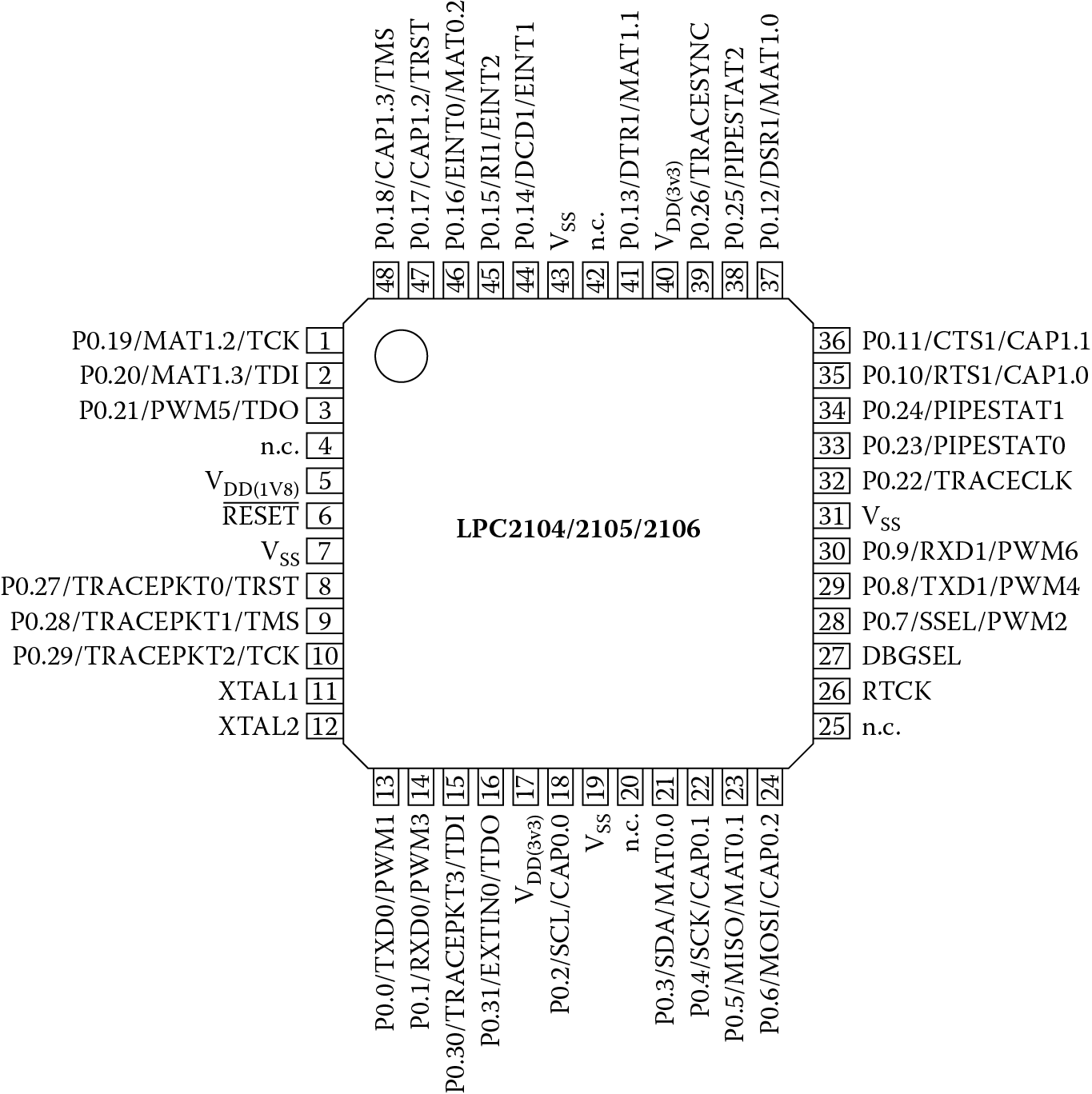
Pin descriptions for the LPC2104. (From Doc. LPC2104–2105–2106–6 Product Data Sheet, NXP Semiconductors, July 2007. With permission.)
LDR r5, = PINSEL0 ; base address of register
LDR r6,[r5] ; get contents
BIC r6,r6,#0xF ; clear out lower nibble
ORR r6,r6,#0x5 ; sets P0.0 to Tx0 and P0.1 to Rx0
STR r6, [r5] ; r/modify/w back to register
The next step to configuring the UART is to set the number of data bits, the parity, and the number of stop bits. Again, the starting address of the UART0 configuration register, 0xE000C000, is loaded into a general register to be used as a base address. The LCR and LSR registers can be accessed using a pre-indexed addressing scheme, where the offsets are equated to known values at the beginning of the final routine. Here, LCR0 would be equated to 0xC, and for our write routine, LSR0 would be equated to 0x14. Since these are 8-bit registers, they must be accessed using STRB and LDRB instructions. The rest of the configuration code is below.
LDR r5, =U0START
MOV r6, #0x83 ; set 8 bits, no parity, 1 stop bit
STRB r6, [r5, #LCR0] ; write control byte to LCR
MOV r6, #0x61 ; 9600 baud @15 MHz VPB clock
STRB r6, [r5] ; store control byte
MOV r6, #3 ; set DLAB = 0
STRB r6, [r5, #LCR0] ; Tx and Rx buffers set up
16.2.4 Writing the Data to the UART
Now that the UART is configured to send and receive data, we can try writing some data out of the part. In this case, we’ll send some character data—the short message “Watson. Come quickly!” The subroutine for this task is written so that the calling routine can send a single character at a time. When the subroutine receives the character, it’s placed into the transmit buffer, but only after the processor checks to ensure the previous character has been transmitted. Who’s reading this data? In the simulation tools, there is a serial window that can accept data from a UART, driving the necessary handshake lines that are normally attached to the receiver. The assembly code for our transmitter routine looks like the following:
LDR r5, =U0START
wait LDRB r6,[r5,#LSR0] ; get status of buffer
CMP r6,#0x20 ; buffer empty?
BEQ wait ; spin until buffer’s empty
STRB r0,[r5]
16.2.5 Putting the Code Together
Now that we have one subroutine to set up our UART and another to send a character, the remaining code will be responsible for reading a sentence from memory, one character at a time, and calling the subroutine to transmit it. A small loop will read a character from memory and test to see whether it is the null terminator for a string, i.e., the value 0. If so, the loop terminates. Otherwise, the subroutine Transmit is called.
The AAPCS allows registers r0 through r3 to be corruptible, and we’ve used registers r5 and r6 in our subroutines. While the code could be written without having to stack any registers (left as an exercise), we’ll go ahead and set the stack pointer to the start of RAM, which is address 0x40000000. The registers used in our subroutines can then be saved off. The code below is a complete routine.
AREA UARTDEMO, CODE, READONLY
PINSEL0 EQU 0xE002C000 ; controls the function of the pins
U0START EQU 0xE000C000 ; start of UART0 registers
LCR0 EQU 0xC ; line control register for UART0
LSR0 EQU 0x14 ; line status register for UART0
RAMSTART EQU 0x40000000 ; start of onboard RAM for 2104
ENTRY
start
LDR sp, = RAMSTART ; set up stack pointer
BL UARTConfig ; initialize/configure UART0
LDR r1, = CharData ; starting address of characters
Loop
LDRB r0, [r1],#1 ; load character, increment address
CMP r0,#0 ; null terminated?
BLNE Transmit ; send character to UART
BNE Loop ; continue if not a ‘0’
done B done ; otherwise we’re done
; Subroutine UARTConfig
; This subroutine configures the I/O pins first. It
; then sets up the UART control register. The
; parameters
; are set to 8 bits, no parity and 1 stop bit.
; Registers used:
; r5 – scratch register
; r6 – scratch register
; inputs: none
; outputs: none
UARTConfig
STMIA sp!, {r5,r6,lr}
LDR r5, = PINSEL0 ; base address of register
LDR r6,[r5] ; get contents
BIC r6,r6,#0xF ; clear out lower nibble
ORR r6,r6,#0x5 ; sets P0.0 to Tx0 and P0.1 to Rx0
STR r6, [r5] ; r/modify/w back to register
LDR r5, = U0START
MOV r6, #0x83 ; set 8 bits, no parity, 1 stop bit
STRB r6, [r5, #LCR0] ; write control byte to LCR
MOV r6, #0x61 ; 9600 baud @15 MHz VPB clock
STRB r6, [r5] ; store control byte
MOV r6, #3 ; set DLAB = 0
STRB r6, [r5, #LCR0] ; Tx and Rx buffers set up
LDMDB sp!,{r5,r6,pc}
; Subroutine Transmit
; This routine puts one byte into the UART
; for transmitting.
; Register used:
; r5 – scratch
; r6 - scratch
; inputs: r0- byte to transmit
; outputs: none
;
Transmit
STMIA sp!,{r5,r6,lr}
LDR r5, = U0START
wait LDRB r6,[r5,#LSR0] ; get status of buffer
CMP r6,#0x20 ; buffer empty?
BEQ wait ; spin until buffer’s empty
STRB r0,[r5]
LDMDB sp!,{r5,r6,pc}
CharData
DCB “Watson. Come quickly!”,0
END
16.2.6 Running the Code
At this point, you should take some time to enter the code and run it in the Keil tools. It should be run in the same manner we have taken with all of the other programs, namely that it starts in memory at address 0x0, and there are no handlers of any kind for exceptions. The tools have additional windows that allow you to view peripherals on the chip. The peripheral we use here, UART0, can be seen by choosing UART0 from the Peripherals menu after the debug session has been started. This will bring up the peripheral window, shown in Figure 16.5.
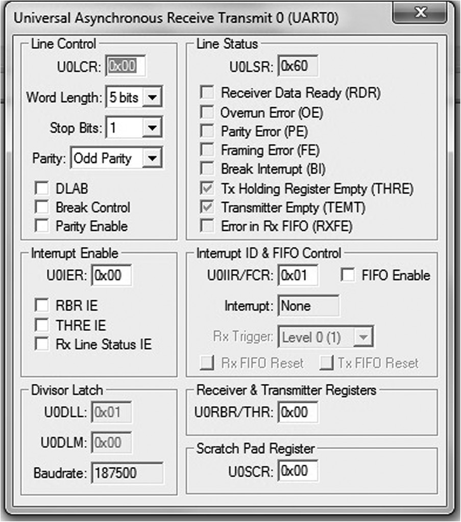
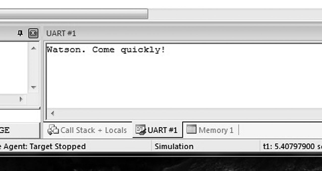
To see the output from the UART, you can use the Serial Window submenu from the View menu on the toolbar. You should select UART #1, which brings up the window shown in Figure 16.6.
16.3 The LPC2132
Figure 16.7 shows a block diagram of the LPC2132 microcontroller, which looks very much like the LPC2104. It has the same ARM7TDMI processor, the same AHB and VPB busses, and a very similar set of peripherals, which is fortunate. With a similar structure and memory map, programming our microcontroller should be very straightforward. The peripheral of interest this time is the D/A converter with its associated output pin AOUT. Since we’ve already covered fractional arithmetic, sine tables, and subroutines, we can tie all of these concepts together by creating a sine wave using the D/A converter. The output AOUT will be monitored on a simulated logic analyzer in the Keil tools so that we can see our sine wave.
LPC2132 block diagram. (From UM10120 Vol. 1: LPC213x User Manual, NXP Semiconductors, June 2006. With permission.)
16.3.1 The D/A Converter
In many signal processing and control applications, an analog waveform is sampled, processed in some way, e.g., a digital filter, and then converted back into an analog waveform. The process of taking a binary value and generating a voltage based on that value requires a digital-to-analog converter. There are many types, including tree networks and R-2R ladders, but their construction lies outside the scope of this book. Fortunately, the electronics can be overlooked for the moment and we can concentrate on using the device.
The basic operation of the D/A converter takes a 10-bit binary value and generates a voltage on AOUT which is proportional to a reference voltage VREF. In other words, if our binary number in base ten is value, then the output voltage is
To use the D/A converter, we will need to set up the pin P0.25 to be our analog output AOUT. Afterward, we can send our 10-bit value to this peripheral to be converted.
16.3.2 The Memory Map
The system memory map for the LPC2132 is shown in Figure 16.8. By now, we recognize the 64 KB of ROM memory from address 0x00000000 to 0x0000FFFF and the 16 KB of RAM starting at address 0x40000000. The peripherals are memory-mapped in high memory, starting at address 0xE0000000. Again, zooming in a bit more, our peripheral has a register called DACR, or DAC Register, which is used for configuring the D/A converter as well as giving it a value to convert. The register is located at address 0xE006C000, and bits [15:6] are the 10 bits of digital input, as shown in Table 16.3.
DAC Register Bit Description
|
Bit |
Symbol |
Value |
Description |
Reset Value |
|
5:0 |
— |
Reserved, user software should not write ones to reserved bits. The value read from a reserved bit is not defined. |
NA |
|
|
15:6 |
VALUE |
After the selected settling time after this field is written with a new VALUE, the voltage on the AOUT pin (with respect to VSSA) is VALUE/1024 * VREF . |
0 |
|
|
16 |
BIAS |
0 |
The settling time of the DAC is 1 μs max, and the maximum current is 700 μA. |
0 |
|
1 |
The settling time of the DAC is 2.5 μs and the maximum current is 350 μA. |
|||
|
31:17 |
— |
Reserved, user software should not write ones to reserved bits. The value read from a reserved bit is not defined. |
NA |
LPC2132 memory map. (From UM10120 Vol. 1: LPC213x User Manual, NXP Semiconductors, June 2006. With permission.)
16.3.3 Configuring the D/A Converter
Before using the D/A converter, we need to configure pin P0.25 such that it becomes AOUT, in the same way we changed the UART pins that were also multiplexed. The code below enables the D/A converter and sets the pin by writing 0b10 to bits [19:18] of the Pin Function Select Register called PINSEL1, which is located at address 0xE002C004. A read-modify-write sequence ensures that other bits that are set or clear are not altered:
LDR r6, = PINSEL1 ; PINSEL1 configures pins
LDR r7,[r6] ; read/modify write
ORR r7,r7,#1:SHL:19 ; set bit 19
BIC r7,r7,#1:SHL:18 ; clear bit 18
STR r7,[r6] ; change P0.25 to Aout
16.3.4 Generating a Sine Wave
The D/A converter will take an unsigned binary value and generate a voltage that ranges between 0 and VREF (in our simulation, this is 3.3V). To see a complete sine wave, all we have to build is a simple loop that counts from 0 to 359. Say this counter is held in register r1. The sine table we built in Chapter 12 will return a Q31 value given the argument in register r1. However, we will have to scale and shift the output of our sine function, so that the value v sent to the D/A converter is
v = 512 × sin(r1) + 512
since sine returns negative arguments in two’s complement. Scaling and shifting the output of our sine table will force v’s range between 0 and 1024, which is what the D/A converter understands. To write the 10-bit value to the DAC Register, a half-word store moves the value v that has been shifted 6 bits so that it sits in bits [15:6]. So, the code would be
ASR r0,r0,#16 ; convert Q31 to Q15
LSL r0,r0,#9 ; x512 now in Q15 notation
ASR r0,r0,#15 ; keep the integer part only
ADD r0,r0,#512 ; 512 x sin(r1) + 512 to show wave
LSL r0,r0,#6 ; bits 5:0 of DAC are undefined
STRH r0,[r8] ; write to DACR
16.3.5 Putting the Code Together
To put everything together, we first convert the sine table to a subroutine, making sure to follow the AAPCS rules for passing arguments, namely to put the argument in register r1 and expect the sine of the argument in register r0. Since registers r4, r5, and r7 were changed in the subroutine, we stack those before using them. While not absolutely necessary, our loop counter counts down rather than up, and we subtract the loop counter from 360 to use as the argument to our sine function. The complete code is shown below.
; Sine wave generator using the LPC2132 microcontroller
; This program will generate a sine wave using
; the D/A converter on the controller. The output can be
; viewed using the Logic Analyzer in the Keil tools.
PINSEL1 EQU 0xE002C004
DACREG EQU 0xE006C000
SRAMBASE EQU 0x40000000
AREA SINEWAVE, CODE
ENTRY
main
LDR sp, = SRAMBASE ; initialize stack pointer
LDR r6, = PINSEL1 ; PINSEL1 configures pins
LDR r8, = DACREG ; DAC Register[15:6] is VALUE
LDR r7,[r6] ; read/modify write
ORR r7,r7,#1:SHL:19 ; set bit 19
BIC r7,r7,#1:SHL:18 ; clear bit 18
STR r7,[r6] ; change P0.25 to Aout
outloop
MOV r6,#360 ; start counter
inloop
RSB r1,r6,#360 ; arg = 360 - loop count
BL sine ; get sin(r1)
; Now that we have r0 = sin(r1), we need to send
; this to the DAC converter.
; First, we take the Q31 value and make it Q15
; and multiply it by 512. Then we offset the result
; by 512 to show the full sine wave. Aout is
; VALUE/1024*Vref, so our sine wave should swing
; between 0 and 3.3 V on the output.
ASR r0,r0,#16 ; convert Q31 to Q15
LSL r0,r0,#9 ; x512 now in Q15 notation
ASR r0,r0,#15 ; keep the integer part only
ADD r0,r0,#512 ; 512 x sin(r1) + 512 to show wave
LSL r0,r0,#6 ; bits 5:0 of DAC are undefined
STRH r0,[r8] ; write to DACR
SUBS r6,r6,#1 ; count down to 0
BNE inloop
B outloop ; do this forever
; Sine function
; Returns Q31 value for integer arguments from 0 to 360
; Registers used:
; r0 = return value in Q31 notation
; r1 = sin argument (in degrees)
; r4 = starting address of sine table
; r5 = temp
; r7 = copy of argument
sine
STMIA sp!,{r4,r5,r7,lr} ; stack used registers
MOV r7, r1 ; make a copy
LDR r5, = 270 ; won’t fit into rotation scheme
ADR r4, sin_data ; load address of sin table
CMP r1, #90 ; determine quadrant
BLE retvalue ; first quadrant?
CMP r1, #180
RSBLE r1,r1,#180 ; second quadrant?
BLE retvalue
CMP r1, r5
SUBLE r1, r1, #180 ; third quadrant?
BLE retvalue
RSB r1, r1, #360 ; otherwise, fourth
retvalue
LDR r0,[r4,r1,LSL #2] ; get sin value from table
CMP r7, #180 ; do we return a neg value?
RSBGT r0, r0, #0 ; negate the value
LDMDB sp!,{r4,r5,r7,pc} ; restore registers
done B done
ALIGN
sin_data
DCD 0x00000000,0x023BE164,0x04779630,0x06B2F1D8
DCD 0x08EDC7B0,0x0B27EB50,0x0D613050,0x0F996A30
DCD 0x11D06CA0,0x14060B80,0x163A1A80,0x186C6DE0
DCD 0x1A9CD9C0,0x1CCB3220,0x1EF74C00,0x2120FB80
DCD 0x234815C0,0x256C6F80,0x278DDE80,0x29AC3780
DCD 0x2BC750C0,0x2DDF0040,0x2FF31BC0,0x32037A40
DCD 0x340FF240,0x36185B00,0x381C8BC0,0x3A1C5C80
DCD 0x3C17A500,0x3E0E3DC0,0x40000000,0x41ECC480
DCD 0x43D46500,0x45B6BB80,0x4793A200,0x496AF400
DCD 0x4B3C8C00,0x4D084600,0x4ECDFF00,0x508D9200
DCD 0x5246DD00,0x53F9BE00,0x55A61280,0x574BB900
DCD 0x58EA9100,0x5A827980,0x5C135380,0x5D9CFF80
DCD 0x5F1F5F00,0x609A5280,0x620DBE80,0x63798500
DCD 0x64DD8900,0x6639B080,0x678DDE80,0x68D9F980
DCD 0x6A1DE700,0x6B598F00,0x6C8CD700,0x6DB7A880
DCD 0x6ED9EC00,0x6FF38A00,0x71046D00,0x720C8080
DCD 0x730BAF00,0x7401E500,0x74EF0F00,0x75D31A80
DCD 0x76ADF600,0x777F9000,0x7847D900,0x7906C080
DCD 0x79BC3880,0x7A683200,0x7B0A9F80,0x7BA37500
DCD 0x7C32A680,0x7CB82880,0x7D33F100,0x7DA5F580
DCD 0x7E0E2E00,0x7E6C9280,0x7EC11A80,0x7F0BC080
DCD 0x7F4C7E80,0x7F834F00,0x7FB02E00,0x7FD31780
DCD 0x7FEC0A00,0x7FFB0280,0x7FFFFFFF
END
16.3.6 Running the Code
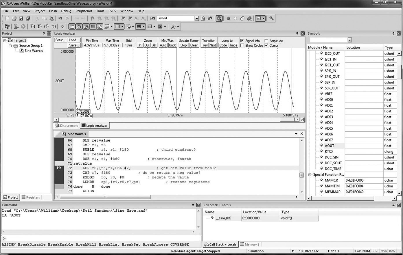
A logic analyzer in the MDK tools allows you to place signals in a window for viewing in the same way that you would probe pins on an actual part. For example, you can take the signal AOUT and drag it into the logic analyzer. As the value changes in real time, you can track it, stopping the processor at any point to read values. After you build a project for this code, enter the program and start the debugger. Open the Symbol window found in the View menu. Expand the Virtual Registers listing to show all of the pins. Open the Logic Analyzer window, also found in the View menu under Analysis Windows. Drag the pin called AOUT into the Logic Analyzer window, then start the simulation. You should see the sine wave, shown in Figure 16.9.
16.4 The Tiva Launchpad
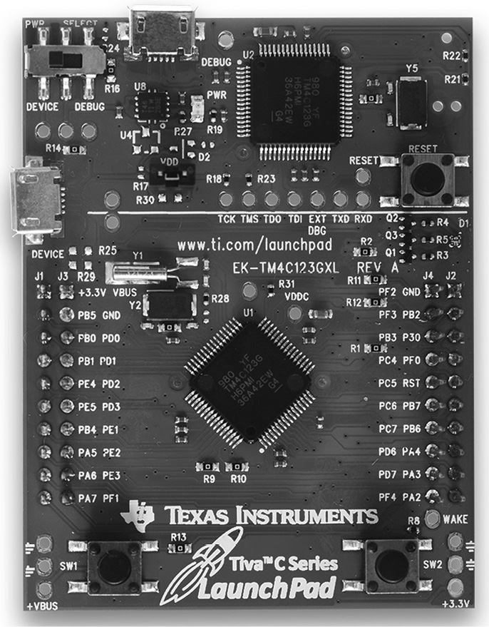
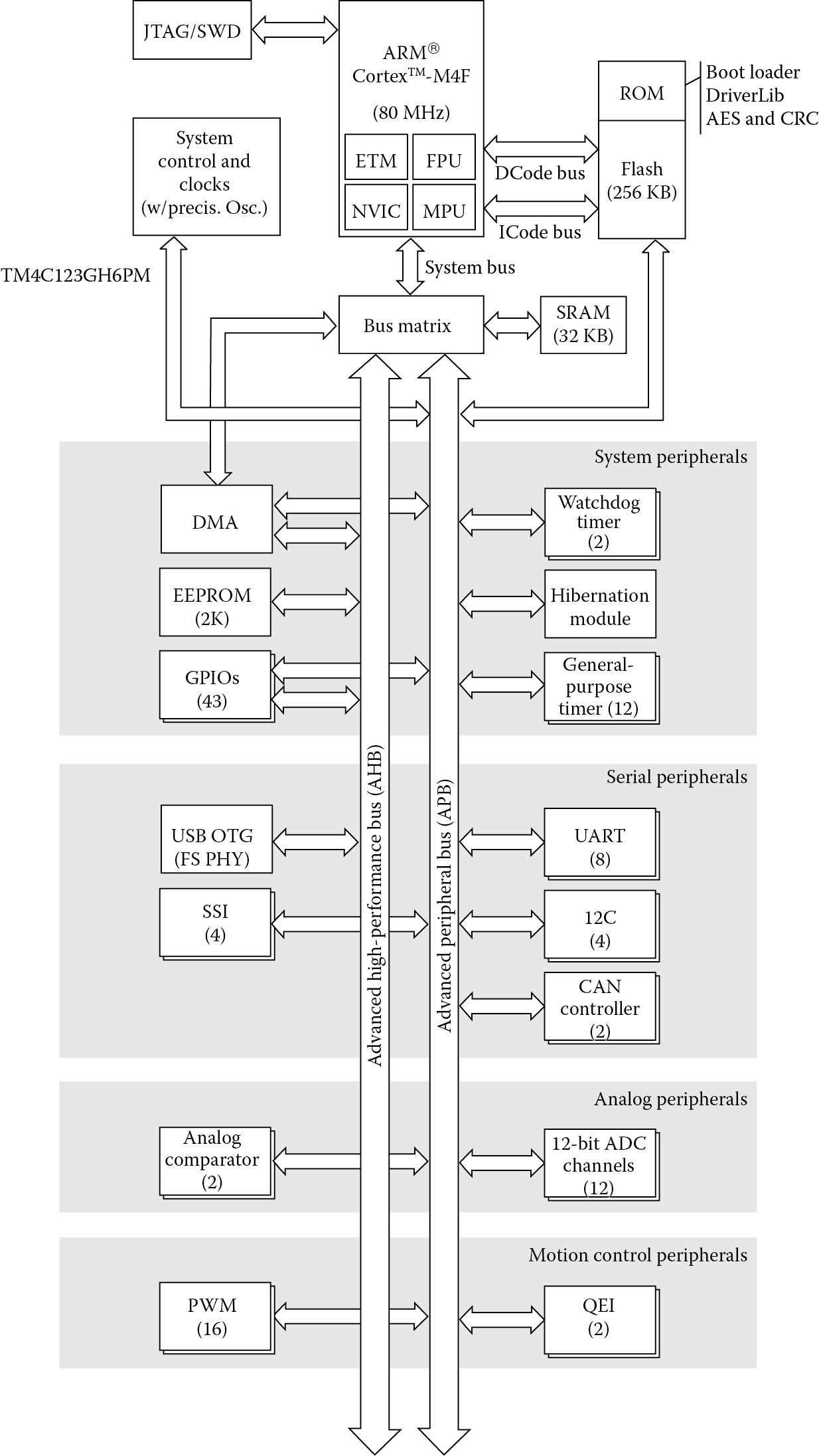
For a bit of variety, as well as a good illustration of using general purpose input and output lines, we’ll turn next to an inexpensive evaluation module from Texas Instruments, shown in Figure 16.10, which contains the TM4C123GH6PM microcontroller. Figure 16.11 shows a block diagram of the microcontroller, which has a similar layout as the other microcontrollers we’ve examined. Rather than an ARM7TDMI core, it uses a Cortex-M4 processor with floating-point hardware, but we will address the peripherals the same way as we did in Sections 16.2 and 16.3. Up until this point, we’ve used simulation models to run our programs; now we’re using real hardware. Using the Code Composer Studio tools, a small block of code can be written to turn on the peripheral, set up the clocks, and then change the color of the LEDs on the board. Note that there are no simulation models of the evaluation module, hence the use of actual hardware.
16.4.1 General-Purpose I/O
General purpose I/O lines are probably the most straightforward of all peripherals to understand, and they can be very versatile. Since they can be configured as either input lines or output lines, you can use them for a variety of applications: driving LEDs or other components in a system, accepting parallel data from another device, or using them as a form of interrupt. Their versatility can sometimes prove to be maddening, mostly due to the sheer volume of documentation available on configuring them. Outputs can have different drive strengths, the GPIO lines might be multiplexed with other peripheral lines, some ports are available on both the AHB and the APB bus, etc. For the complete list of registers and options, refer to the Tiva TM4C123GH6PM Data Sheet (Texas Instruments 2013c), but for now, let’s examine a (relatively) simple, short block of code to see how everything is configured.
16.4.2 The Memory Map
There are, in fact, so many memory-mapped registers on the TM4C123GH6PM that it’s sometimes difficult to know which ones to use. In order to set up the clocks and the PLL so that our evaluation module actually runs code, we will need to configure the Run-Mode Clock Configuration (RCC) Register, which is part of the System Control Registers, which have a base address of 0x400FE000. The entire sequence for setting up the clocks is listed in Section 16.4.5. In order to use the GPIO port, it must be enabled by turning on its clock, which is configured in the General-Purpose Input/Output Run Mode Clock Gating Control (RCGCGPIO) Register. Yes, it’s a mouthful. Luckily, it has the same base address as the RCC Register, but its offset is 0x608. The code looks like:
; Enable GPIOF
; RCGCGPIO (page 339)
MOVW r2, #0x608 ; offset for this register
LDR r1, [r0, r2] ; grab the register contents
ORR r1, r1, #0x20 ; enable GPIOF clock
STR r1, [r0, r2]
According to the data sheet, there must be a delay of 3 system clocks after the GPIO module clock is enabled before any GPIO module registers are accessed. There are four instructions between the STR that enables the clock and the STR that sets the direction of the port, satisfying this requirement.
16.4.3 Configuring the GPIO Pins
Moving into a different memory space, the GPIO port itself is configured through dedicated registers. Table 16.4 shows the location of each of the GPIO ports on the TM4C123GH6PM. The LED is actually located on APB bus Port F, so our base address will be 0x40025000. We’ll set the direction of GPIO Port F lines 1, 2, and 3 to be outputs:
GPIO Port Locations
|
Port |
Address |
|
|
APB Bus |
GPIO Port A |
0x40004000 |
|
GPIO Port B |
0x40005000 |
|
|
GPIO Port C |
0x40006000 |
|
|
GPIO Port D |
0x40007000 |
|
|
GPIO Port E |
0x40024000 |
|
|
GPIO Port F |
0x40025000 |
|
|
AHB Bus |
GPIO Port A |
0x40058000 |
|
GPIO Port B |
0x40059000 |
|
|
GPIO Port C |
0x4005A000 |
|
|
GPIO Port D |
0x4005B000 |
|
|
GPIO Port E |
0x4005C000 |
|
|
GPIO Port F |
0x4005D000 |
; Set the direction using GPIODIR (page 661)
; Base is 0x40025000
MOVW r0, #0x5000
MOVT r0, #0x4002
MOVW r2, #0x400 ; offset for this register
MOV r1, #0xE
STR r1, [r0, r2] ; set 1 or 2 or 3 for output
If you are using the Keil tools, the constant 0x40025000 can be loaded into register r0 with an LDR pseudo-instruction from Chapter 6; however, the Code Composer Studio assembler does not support this, so two separate move instructions will do the trick. There’s an additional level of gating on the port—the GPIO Digital Enable Register will need to be configured:
; set the GPIODEN lines
MOVW r2, #0x51c ; offset for this register
STR r1, [r0, r2] ; set 1 and 2 and 3 for I/O
16.4.4 Turning on the LEDs
The Tiva Launchpad board has a multi-colored LED that is controlled through three GPIO lines on Port F, one for red, one for green, and one for blue. The red LED is attached to line PF1, the green LED is attached to line PF2, and the blue LED is attached to line PF3. Now that Port F has been enabled and the appropriate lines have been configured as outputs, we can light the LEDs by driving a 1 to the GPIO line of our choice. To showcase all three colors, we can create a loop that selects one color at a time, cycling through all three by changing the value being written to the port.
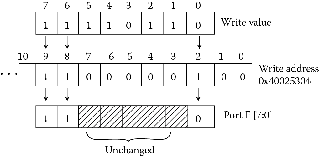
In Chapter 5, the concept of bit-banding allowed individual bits of a memory-mapped register to be accessed using a single read or write operation. It turns out the a similar feature is available on the TM4C123GH6PM microcontroller for accessing GPIO lines, where the address is used as a mask, as shown in Figure 16.12. For example, suppose we wish to alter only bits [7:6] and bit [0] of GPIO Port F. We can use bits [9:2] of the address in our write operation to form a bit mask, so that instead of writing to the base address of Port F (0x40025000), we would store our value to address (0x40025304). Now that our mask is in place, no matter what value we write to the port, such as 0xF6, only bits [7:6] and [0] are altered. Specifically for our LED example, we wish to have bits [9:2] of the address be 0b00111000, or 0x38, since we only want to change the LED lines connected to Port F. This value becomes our offset.
The following code shows our loop, complete with a small delay to give the observer a chance to see the individual colors of the LED. The delay value of 0xF40000 is arbitrary, but at 16 MHz, it gives us about 1 second to view a single color.
SUB r7, r7, r7 ; clear out r7
MOV r6, #2 ; start with LED = 0b10
mainloop
; turn on the LED
; if bits [9:2] affect the writes, then the address
; is offset by 0x38
STR r6, [r0, #0x38] ; base + 0x38 so [9:2] = 0b111000
MOVT r7, #0xF4 ; set counter to 0xF40000
spin
SUBS r7, r7, #1
BNE spin
; change colors
CMP r6, #8
ITE LT
LSLLT r6, r6, #1 ; LED = LED * 2
MOVGE r6, #2 ; reset to 2 otherwise
B mainloop
The first line of our code sets the value to be written to Port F to 0b0010, and we plan to cycle through the values 0b0100, 0b1000, then back to 0b0010. The STR instruction will use the same base address in register r0 that we used earlier to configure the port, only the offset has now changed to our mask value. By using a MOVT instruction to store a value in the top half of register r7, we can load the value 0xF40000 without shifting any bits. The spin loop then does nothing but subtract one from the counter value until it expires. Once the loop reaches zero, the color is changed by logically shifting left the value to be stored to the port. If the value is equal to 0b1000, then it is reset to 0b0010 and the code branches to the start of the main loop.
16.4.5 Putting the Code Together
The entire program to control the LEDs is listed below. If you follow the suggestions outlined in Appendix A for using the Code Composer Studio tools, this code should assemble without any issues.
myStart:
; Set sysclk to DIV/4, use PLL, XTAL_16 MHz, OSC_MAIN
; system control base is 0x400FE000, offset 0x60
; bits[26:23]= 0x3
; bit[22] = 0x1
; bit[13] = 0x0
; bit[11] = 0x0
; bits[10:6] = 0x15
; bits[5:4] = 0x0
; bit[0] = 0x0
; This all translates to a value of 0x01C00540
MOVW r0, #0xE000
MOVT r0, #0x400F
MOVW r2, #0x60 ; offset 0x60 for this register
MOVW r1, #0x0540
MOVT r1, #0x01C0
STR r1, [r0, r2] ; write the register’s contents
; Enable GPIOF
; RCGCGPIO (page 339)
MOVW r2, #0x608 ; offset for this register
LDR r1, [r0, r2] ; grab the register contents
ORR r1, r1, #0x20 ; enable GPIOF clock
STR r1, [r0, r2]
; Set the direction using GPIODIR (page 661)
; Base is 0x40025000
MOVW r0, #0x5000
MOVT r0, #0x4002
MOVW r2, #0x400 ; offset for this register
MOV r1, #0xE
STR r1, [r0, r2] ; set 1 or 2 or 3 for output
;set the GPIODEN lines
MOVW r2, #0x51c ; offset for this register
STR r1, [r0, r2] ; set 1 and 2 and 3 for I/O
SUB r7, r7, r7 ; clear out r7
MOV r6, #2 ; start with LED = 0b10
mainloop
; turn on the LED
; if bits [9:2] affect the writes, then the address
; is offset by 0x38
STR r6, [r0, #0x38] ; base + 0x38 so [9:2] = 0b00111000
MOVT r7, #0xF4 ; set counter to 0xF40000
spin
SUBS r7, r7, #1
BNE spin
; change colors
CMP r6, #8
ITE LT
LSLLT r6, r6, #1 ; LED = LED * 2
MOVGE r6, #2 ; reset to 2 otherwise
B mainloop
16.4.6 Running the Code
The Code Composer Studio tools will help you build a project, enter the assembly code into a file, then run the code on the Launchpad evaluation module. The code will be loaded into Flash memory, so that once you build your project, in the future, once power is applied to the board, the same program will immediately execute and you should see the LEDs continue to flash. Take some time to set breakpoints on code segments to see how the register values change, and experiment with different delay values for the loop. Obviously you can restore the evaluation module’s default program if you wish using the tools provided by Texas Instruments.
16.5 Exercises
- Write an SVC handler so that when an SVC instruction is executed, the handler prints out the contents of register r8. The program should incorporate assembly routines similar to the ones already built. For example, you will need to convert the binary value in register r8 to ASCII first, then use a UART to display the information in the Keil tools. Have the routine display “Register r8 =” followed by the register’s value.
- Choose a device with general-purpose I/O pins, such as the LPC2103, and write an assembly routine that sequentially walks a 1 back and forth across the I/O pins. In other words, at any given time, only a single pin is set to 1—all others are 0. Set up the Keil tools to display the pins (you might want to compile and run the Blinky example that comes with the tools to see what the interface looks like).
- Rewrite the two examples described in Section 16.2.5 and Section 16.3.5 using full descending stacks.
- What is the address range for on-chip SRAM for the LPC2106 microcontroller?
- Write an assembly program that takes a character entered from a keyboard and echoes it to a display. To do this, you will need to use two UARTs, one for entering data and one for displaying it. The routine that accepts characters should not generate an interrupt when data is available, but merely wait for the character to appear in its buffer. In other words, the UART routine should spin in a loop until a key is pressed, after which it branches back to the main routine. Note that the UART window must have the focus in order to accept data from a keyboard (this is a Windows requirement), so be sure to click on the UART window first when testing your code.
- Using the D/A converter example as a guide, write an assembly routine that will generate a waveform defined by
f(x) = asin(0.5x) + bsin(x) + c
- where a, b, and c are constants that allow a full period to be displayed. The output waveform should appear on AOUT so that you can view it on the logic analyzer in the Keil tools.
- What is the address range for the following devices on the LPC2132 microcontroller?
- General-purpose input/output ports
- Universal asynchronous receiver transmitter 0
- Analog-to-digital converter
- Digital-to-analog converter
- What is the address range for the following devices on the STR910FM32 microcontroller?
- General-purpose input/output ports
- Real time clock
- Universal asynchronous receiver transmitter
- Analog-to-digital converter
- The UART example given in this chapter uses registers r5 and r6 to configure the UART and, therefore, must write them to the stack before corrupting them. Rewrite the UART example so that no registers are stacked and the routine is still AAPCS compliant.
- Modify the routine in Section 16.4.5 so that the LEDs flash alternately between red and blue for about 1 second each.