Table of Contents for
ARM Assembly Language, 2nd Edition
 ARM Assembly Language, 2nd Edition
Published by
Chapman and Hall/CRC, 2016
ARM Assembly Language, 2nd Edition
Published by
Chapman and Hall/CRC, 2016
- Contents
- ARM Assembly Language: Fundamentals and Techniques, Second Edition
- Preliminaries
- To our families
- Preface
- Acknowledgments
- Authors
- Chapter 1 - An Overview of Computing Systems
- Chapter 2 - The Programmer’s Model
- Chapter 3 - Introduction to Instruction Sets: v4T and v7-M
- Chapter 4 - Assembler Rules and Directives
- Chapter 5 - Loads, Stores, and Addressing
- Chapter 6 - Constants and Literal Pools
- Chapter 7 - Integer Logic and Arithmetic
- Chapter 8 - Branches and Loops
- Chapter 9 - Introduction to Floating-Point: Basics, Data Types, and Data Transfer
- Chapter 10 - Introduction to Floating-Point: Rounding and Exceptions
- Chapter 11 - Floating-Point Data-Processing Instructions
- Chapter 12 - Tables
- Chapter 13 - Subroutines and Stacks
- Chapter 14 - Exception Handling: ARM7TDMI
- Chapter 15 - Exception Handling: v7-M
- Chapter 16 - Memory-Mapped Peripherals
- Chapter 17 - ARM, Thumb and Thumb-2 Instructions
- Chapter 18 - Mixing C and Assembly
- Appendix A: Running Code Composer Studio
- Appendix B: Running Keil Tools
- Appendix C: ASCII Character Codes
- Appendix D
- Glossary
- References
Chapter 5
Loads, Stores, and Addressing
5.1 Introduction
Processor architects spend a great deal of time analyzing typical routines on simulation models of a processor, often to find performance bottlenecks. Dynamic instruction usage gives a good indication of the types of operations that are performed the most while code is running. This differs from static usage that only describes the frequency of an instruction in the code itself. It turns out that while typical code is running, about half of the instructions deal with data movement, including data movement between registers and memory. Therefore, loading and storing data efficiently is critical to optimizing processor performance. As with all RISC processors, dedicated instructions are required for loading data from memory and storing data to memory. This chapter looks at those basic load and store instructions, their addressing modes, and their uses.
5.2 Memory
Earlier we said that one of the major components of any computing system is memory, a place to store our data and programs. Memory can be conceptually viewed as contiguous storage elements that hold data, each element holding a fixed number of bits and having an address. The typical analogy for memory is a very long string of mailboxes, where data (your letter) is stored in a box with a specific number on it. While there are some digital signal processors that use memory widths of 16 bits, the system that is nearly universally adopted these days has the width of each element as 8 bits, or a byte long. Therefore, we always refer to memory as being so many megabytes* (abbreviated MB, representing 220 or approximately 106 bytes), gigabytes (abbreviated GB, representing 230 or approximately 109 bytes), or even terabytes (abbreviated TB, representing 240 or approximately 1012 bytes).
Younger programmers really should see what an 80 MB hard drive used to look like as late as the 1980s—imagine a washing machine with large, magnetic plates in the center that spun at high speeds. With the advances in magnetic materials and silicon memories, today’s programmers have 4 TB hard drives on their desks and think nothing of it! Visit museums or universities with collections of older computers, if only to appreciate how radically storage technology has changed in less than one lifetime.
In large computing systems, such as workstations and mainframes, the memory to which the processor speaks directly is a fixed size, such as 4 GB, but the machine is capable of swapping out areas of memory, or pages, to larger storage devices, such as hard drives, that can hold as much as a terabyte or more. The method that is used to do this lies outside the scope of this book, but most textbooks on computer architecture cover it pretty well. Embedded systems typically need far less storage, so it’s not uncommon to see a complete design using 2 MB of memory or less. In an embedded system, one can also ask how much memory is actually needed, since we may only have a simple task to perform with very little data. If our processor is used in an application that takes remote sensor data and does nothing but transmit it to a receiver, what could we possibly need memory for, other than storing a small program or buffering small amounts of data? Often, it turns out, embedded processors spend a lot of time twiddling their metaphorical thumbs, idly waiting for something to do. If a processor such as one in our remote sensor does decide to shut down or go into a quiescent state, it may have to save off the contents of its registers, including control registers, floating-point registers, and status registers. Energy management software may decide to power down certain parts of a chip when idle, and a loss of power may mean a loss of data. It may even have to store the contents of other on-chip memories such as a cache or tightly coupled memory (TCM).
Memory comes in different flavors and may reside at different addresses. For example, not all memory has to be readable and writable—some may be readable only, such as ROM (Read-Only Memory) or EEPROM (Electrically Erasable Programmable ROM)—but the data is accessed the same way for all types of memory. Embedded systems often use less expensive memories, e.g., 8-bit memory over faster, more expensive 32-bit memory, and it is left to the hardware designers to build a memory system for the application at hand. Programmers then write code for the system knowing something about the hardware up front. In fact, maps are often made of the memory system so that programmers know exactly how to access the various memory types in the system. Examining Figure 1.4 again, you’ll notice that the address bus on the ARM7TDMI consists of 32 bits, meaning that you could address bytes in memory from address 0 to 232–1, or 4,294,967,295 (0xFFFFFFFF), which is considered to be 4 GB of memory space. If you look at the memory map of a Cortex-M4-based microcontroller, such as the Tiva TM4C123GH6ZRB shown in Table 5.1, you’ll note that the entire address space is defined, but certain address ranges do not exist, such as addresses between 0x44000000 and 0xDFFFFFFF. You can also see that this part has different types of memories on the die—flash ROM memory and SRAM—and an interface to talk to external memory off-chip, such as DRAM. Not all addresses are used, and much of the memory map contains areas dedicated to specific functions, some of which we’ll examine further in later chapters. While the memory layout is defined by an SoC’s implementation, it is not part of the processor core.
Memory Map of the Tiva TM4C123GH6ZRB
|
Start |
End |
Description |
For Details, See Page…a |
Memory |
|||
|
0x0000.0000 |
0x0003.FFFF |
On-chip flash |
553 |
|
0x0004.0000 |
0x00FF.FFFF |
Reserved |
— |
|
0x0100.0000 |
0x1FFF.FFFF |
Reserved for ROM |
538 |
|
0x2000.0000 |
0x2000.7FFF |
Bit-banded on-chip SRAM |
537 |
|
0x2000.8000 |
0x21FF.FFFF |
Reserved |
— |
|
0x2200.0000 |
0x220F.FFFF |
Bit-band alias of bit-banded on-chip SRAM starting at 0x2000.0000 |
537 |
|
0x2210.0000 |
0x3FFF.FFFF |
Reserved |
— |
Peripherals |
|||
|
0x4000.0000 |
0x4000.0FFF |
Watchdog timer 0 |
798 |
|
0x4000.1000 |
0x4000.1FFF |
Watchdog timer 1 |
798 |
|
0x4000.2000 |
0x4000.3FFF |
Reserved |
— |
|
0x4000.4000 |
0x4000.4FFF |
GPIO Port A |
675 |
|
0x4000.5000 |
0x4000.5FFF |
GPIO Port B |
675 |
|
0x4000.6000 |
0x4000.6FFF |
GPIO Port C |
675 |
|
0x4000.7000 |
0x4000.7FFF |
GPIO Port D |
675 |
|
0x4000.8000 |
0x4000.8FFF |
SSI 0 |
994 |
|
0x4000.9000 |
0x4000.9FFF |
SSI 1 |
994 |
|
0x4000.A000 |
0x4000.AFFF |
SSI 2 |
994 |
|
0x4000.B000 |
0x4000.BFFF |
SSI 3 |
994 |
|
0x4000.C000 |
0x4000.CFFF |
UART 0 |
931 |
|
0x4000.D000 |
0x4000.DFFF |
UART 1 |
931 |
|
0x4000.E000 |
0x4000.EFFF |
UART 2 |
931 |
|
0x4000.F000 |
0x4000.FFFF |
UART 3 |
931 |
|
0x4001.0000 |
0x4001.0FFF |
UART 4 |
931 |
|
0x4001.1000 |
0x4001.1FFF |
UART 5 |
931 |
|
0x4001.2000 |
0x4001.2FFF |
UART 6 |
931 |
|
0x4001.3000 |
0x4001.3FFF |
UART 7 |
931 |
|
0x4001.4000 |
0x4001.FFFF |
Reserved |
— |
Peripherals |
|||
|
0x4002.0000 |
0x4002.0FFF |
I2 C 0 |
1044 |
|
0x4002.1000 |
0x4002.1FFF |
I2 C 1 |
1044 |
|
0x4002.2000 |
0x4002.2FFF |
I2 C 2 |
1044 |
|
0x4002.3000 |
0x4002.3FFF |
I2 C 3 |
1044 |
|
0x4002.4000 |
0x4002.4FFF |
GPIO Port E |
675 |
|
0x4002.5000 |
0x4002.5FFF |
GPIO Port F |
675 |
|
0x4002.6000 |
0x4002.6FFF |
GPIO Port G |
675 |
|
0x4002.7000 |
0x4002.7FFF |
GPIO Port H |
675 |
|
0x4002.8000 |
0x4002.8FFF |
PWM 0 |
1270 |
|
0x4002.9000 |
0x4002.9FFF |
PWM 1 |
1270 |
|
0x4002.A000 |
0x4002.BFFF |
Reserved |
— |
|
0x4002.C000 |
0x4002.CFFF |
QEI 0 |
1341 |
|
0x4002.D000 |
0x4002.DFFF |
QEI 1 |
1341 |
|
0x4002.E000 |
0x4002.FFFF |
Reserved |
— |
|
0x4003.0000 |
0x4003.0FFF |
16/32-bit Timer 0 |
747 |
|
0x4003.1000 |
0x4003.1FFF |
16/32-bit Timer 1 |
747 |
|
0x4003.2000 |
0x4003.2FFF |
16/32-bit Timer 2 |
747 |
|
0x4003.3000 |
0x4003.3FFF |
16/32-bit Timer 3 |
747 |
|
0x4003.4000 |
0x4003.4FFF |
16/32-bit Timer 4 |
747 |
|
0x4003.5000 |
0x4003.5FFF |
16/32-bit Timer 5 |
747 |
|
0x4003.6000 |
0x4003.6FFF |
32/64-bit Timer 0 |
747 |
|
0x4003.7000 |
0x4003.7FFF |
32/64-bit Timer 1 |
747 |
|
0x4003.8000 |
0x4003.8FFF |
ADC 0 |
841 |
|
0x4003.9000 |
0x4003.9FFF |
ADC 1 |
841 |
|
0x4003.A000 |
0x4003.BFFF |
Reserved |
— |
|
0x4003.C000 |
0x4003.CFFF |
Analog Comparators |
1240 |
|
0x4003.D000 |
0x4003.DFFF |
GPIO Port J |
675 |
|
0x4003.E000 |
0x4003.FFFF |
Reserved |
— |
|
0x4004.0000 |
0x4004.0FFF |
CAN 0 Controller |
1094 |
|
0x4004.1000 |
0x4004.1FFF |
CAN 1 Controller |
1094 |
|
0x4004.2000 |
0x4004.BFFF |
Reserved |
— |
|
0x4004.C000 |
0x4004.CFFF |
32/64-bit Timer 2 |
747 |
|
0x4004.D000 |
0x4004.DFFF |
32/64-bit Timer 3 |
747 |
|
0x4004.E000 |
0x4004.EFFF |
32/64-bit Timer 4 |
747 |
|
0x4004.F000 |
0x4004.FFFF |
32/64-bit Timer 5 |
747 |
|
0x4005.0000 |
0x4005.0FFF |
USB |
1146 |
|
0x4005.1000 |
0x4005.7FFF |
Reserved |
— |
|
0x4005.8000 |
0x4005.8FFF |
GPIO Port A (AHB aperture) |
675 |
|
0x4005.9000 |
0x4005.9FFF |
GPIO Port B (AHB aperture) |
675 |
|
0x4005.A000 |
0x4005.AFFF |
GPIO Port C (AHB aperture) |
675 |
|
0x4005.B000 |
0x4005.BFFF |
GPIO Port D (AHB aperture) |
675 |
|
0x4005.C000 |
0x4005.CFFF |
GPIO Port E (AHB aperture) |
675 |
|
0x4005.D000 |
0x4005.DFFF |
GPIO Port F (AHB aperture) |
675 |
|
0x4005.E000 |
0x4005.EFFF |
GPIO Port G (AHB aperture) |
675 |
|
0x4005.F000 |
0x4005.FFFF |
GPIO Port H (AHB aperture) |
675 |
|
0x4006.0000 |
0x4006.0FFF |
GPIO Port J (AHB aperture) |
675 |
|
0x4006.1000 |
0x4006.1FFF |
GPIO Port K (AHB aperture) |
675 |
|
0x4006.2000 |
0x4006.2FFF |
GPIO Port L (AHB aperture) |
675 |
|
0x4006.3000 |
0x4006.3FFF |
GPIO Port M (AHB aperture) |
675 |
|
0x4006.4000 |
0x4006.4FFF |
GPIO Port N (AHB aperture) |
675 |
|
0x4006.5000 |
0x4006.5FFF |
GPIO Port P (AHB aperture) |
675 |
|
0x4006.6000 |
0x4006.6FFF |
GPIO Port Q (AHB aperture) |
675 |
|
0x4006.7000 |
0x400A.EFFF |
Reserved |
— |
|
0x400A.F000 |
0x400A.FFFF |
EEPROM and Key Locker |
571 |
|
0x400B.0000 |
0x400B.FFFF |
Reserved |
— |
|
0x400C.0000 |
0x400C.0FFF |
I2 C 4 |
1044 |
|
0x400C.1000 |
0x400C.1FFF |
I2 C 5 |
1044 |
|
0x400C.2000 |
0x400F.8FFF |
Reserved |
— |
|
0x400F.9000 |
0x400F.9FFF |
System Exception Module |
497 |
|
0x400F.A000 |
0x400F.BFFF |
Reserved |
— |
|
0x400F.C000 |
0x400F.CFFF |
Hibernation Module |
518 |
|
0x400F.D000 |
0x400F.DFFF |
Flash memory control |
553 |
|
0x400F.E000 |
0x400F.EFFF |
System control |
237 |
|
0x400F.F000 |
0x400F.FFFF |
µDMA |
618 |
|
0x4010.0000 |
0x41FF.FFFF |
Reserved |
— |
|
0x4200.0000 |
0x43FF.FFFF |
Bit-banded alias of 0x4000.0000 through 0x400F.FFFF |
— |
|
0x4400.0000 |
0xDFFF.FFFF |
Reserved |
— |
Private Peripheral Bus |
|||
|
0xE000.0000 |
0xE000.0FFF |
Instrumentation Trace Macrocell (ITM) |
70 |
|
0xE000.1000 |
0xE000.1FFF |
Data Watchpoint and Trace (DWT) |
70 |
|
0xE000.2000 |
0xE000.2FFF |
Flash Patch and Breakpoint (FPS) |
70 |
|
0xE000.3000 |
0xE000.DFFF |
Reserved |
— |
|
0xE000.E000 |
0xE000.EFFF |
Cortex-M4F Peripherals (SysTick, NVIC, MPU, FPU and SCB) |
134 |
|
0xE000.F000 |
0xE003.FFFF |
Reserved |
— |
|
0xE004.0000 |
0xE004.0FFF |
Trace Port Interface Unit (TPIU) |
71 |
|
0xE004.1000 |
0xE004.1FFF |
Embedded Trace Macrocell (ETM) |
70 |
|
0xE004.2000 |
0xFFFF.FFFF |
Reserved |
— |
a See Tiva TM4C123GH6ZRB Microcontroller Data Sheet.
5.3 Loads and Stores: The Instructions
Now that we have some idea of how memory is described in the system, the next step is to consider getting data out of memory and into a register, and vice versa. Recall that RISC architectures are considered to be load/store architectures, meaning that data in external memory must be brought into the processor using an instruction. Operations that take a value in memory, multiply it by a coefficient, add it to another register, and then store the result back to memory with only a single instruction do not exist. For hardware designers, this is considered to be a very good thing, since some older architectures had so many options and modes for loading and storing data that it became nearly impossible to build the processors without introducing errors in the logic. Without listing every combination, Table 5.2 describes the most common instructions for dedicated load and store operations in the version 4T and version 7-M instruction sets.
Most Often Used Load/Store Instructions
|
Loads |
Stores |
Size and Type |
|
LDR |
STR |
Word (32 bits) |
|
LDRB |
STRB |
Byte (8 bits) |
|
LDRH |
STRH |
Halfword (16 bits) |
|
LDRSB |
Signed byte |
|
|
LDRSH |
Signed halfword |
|
|
LDM |
STM |
Multiple words |
Load instructions take a single value from memory and write it to a general-purpose register. Store instructions read a value from a general-purpose register and store it to memory. Load and store instructions have a single instruction format:
LDR|STR{<size>}{<cond>} <Rd>, <addressing_mode>
where <size> is an optional size such as byte or halfword (word is the default size), <cond> is an optional condition to be discussed in Chapter 8, and <Rd> is the source or destination register. Most registers can be used for both load and store instructions; however, there are register restrictions in the v7-M instructions, and for version 4T instructions, loads to register r15 (the PC) must be used with caution, as this could result in changing the flow of instruction execution. The addressing modes allowed are actually quite flexible, as we’ll see in the next section, and they have two things in common: a base register and an (optional) offset. For example, the instruction
LDR r9, [r12, r8, LSL #2]
would have a base register of r12 and an offset value created by shifting register r8 left by two bits. We’ll get to the details of shift operations in Chapter 7, but for now just recognize LSL as a logical shift left by a certain number of bits. The offset is added to the base register to create the effective address for the load in this case.
It may be helpful at this point to introduce some nomenclature for the address—the term effective address is often used to describe the final address created from values in the various registers, with offsets and/or shifts. For example, in the instruction above, if the base register r12 contained the value 0x4000 and we added register r8, the offset, which contained 0x20, to it, we would have an effective address of 0x4080 (remember the offset is shifted). This is the address used to access memory. A shorthand notation for this is ea<operands>, so if we said ea<r12 + r8*4>, the effective address is the value obtained from summing the contents of register r12 and 4 times the contents of register r8.
Sifting through all of the options for loads and stores, there are basically two main types of addressing modes available with variations, both of which are covered in the next section:
- Pre-indexed addressing
- Post-indexed addressing
If you allow for the fact that a simple load such as
LDR r2, [r3]
can be viewed as special case of pre-indexed addressing with a zero offset, then loads and stores for the ARM7TDMI and Cortex-M4 processors take the form of an instruction with one of the two indexing schemes. Referring back to Table 5.2, the first three types of instructions simply transfer a word, halfword, or byte to memory from a register, or from memory to a register. For halfword loads, the data is placed in the least significant halfword (bits [15:0]) of the register with zeros in the upper 16 bits. For halfword stores, the data is taken from the least significant halfword. For byte loads, the data is placed in the least significant byte (bits [7:0]) of the register with zeros in the upper 24 bits. For byte stores, the data is taken from the least significant byte.
Example 5.1
Consider the instruction
LDRH r11, [r0]; load a halfword into r11
Assuming the address in register r0 is 0x8000, before and after the instruction is executed, the data appears as follows:
|
Memory |
Address |
|
|
r11 before load |
0xEE |
0x8000 |
|
0x12345678 |
0xFF |
0x8001 |
|
r11 after load |
0x90 |
0x8002 |
|
0x0000FFEE |
0xA7 |
0x8003 |
Notice that 0xEE, the least significant byte at address 0x8000, is moved to the least significant byte in register r11, the second least significant byte, 0xFF, is moved to second least significant byte of register r11, etc. We’ll have much more to say about this ordering shortly.
Signed halfword and signed byte load instructions deserve a little more explanation. The operation itself is quite easy—a byte or a halfword is read from memory, sign extended to 32 bits, then stored in a register. Here the programmer is specifically branding the data as signed data.
Example 5.2
The instruction
LDRSH r11, [r0]; load signed halfword into r11
would produce the following scenario, again assuming register r0 contains the address 0x8000:
|
Memory |
Address |
|
|
r11 before load |
0xEE |
0x8000 |
|
0x12345678 |
0x8C |
0x8001 |
|
r11 after load |
0x90 |
0x8002 |
|
0xFFFF8CEE |
0xA7 |
0x8003 |
As in Example 5.1, the two bytes from memory are moved into register r11, except the most significant bit of the value at address 0x8001, 0x8C, is set, meaning that in a two’s complement representation, this is a negative number. Therefore, the sign bit should be extended, which produces the value 0xFFFF8CEE in register r11.
You may not have noticed the absence of signed stores of halfwords or bytes into memory. After a little thinking, you might come to the conclusion that data stored to memory never needs to be sign extended. Computers simply treat data as a sequence of bit patterns and must be told how to interpret numbers. The value 0xEE could be a small, positive number, or it could be an 8-bit, two’s complement representation of the number -18. The LDRSB and LDRSH instructions provide a way for the programmer to tell the machine that we are treating the values read from memory as signed numbers. This subject will be brought up again in Chapter 7 when we deal with fractional notations.
There are some very minor differences in the two broad classes of loads and stores, for both the ARM7TDMI and the Cortex-M4. For example, those instructions transferring words and unsigned bytes have more addressing mode options than instructions transferring halfwords and signed bytes, as shown in Table 5.3 and Table 5.4. These are not critical to understanding the instructions, so we’ll proceed to see how they are used first.
Addressing Options for Loads and Stores on the ARM7TDMI
|
Imm Offset |
Reg Offset |
Scaled Reg Offset |
Examples |
|
|
Word |
12 bits |
Supported |
Supported |
LDR r0, [r8, r2, LSL #28] |
|
Unsigned byte |
LDRB r4, [r8, #0xF1A] |
|||
|
Halfword |
8 bits |
Supported |
Not supported |
STRH r9, [r10, #0xF4] |
|
Signed halfword |
LDRSB r9, [r2, r1] |
|||
|
Signed byte |
Addressing Options for Loads and Stores on the Cortex-M4
|
Imm Offset |
Reg Offset |
Scaled Reg Offset |
Examples |
|
|
Unsigned byte Signed byte |
Depending on instruction, index can range from −255 to 4095a |
LDRSB r3, [r6, r7, LSL #2] LDRSH r10, [r2, #0x42] STRH r3, [r6, r8] |
||
|
Halfword |
Supported |
Supported |
||
|
Signed halfword |
||||
|
Word |
a Due to the way the instructions are encoded, there are actually differen t instructions for LDRSB r3, [r4, #0] and LDRSB r3, [r4, #-0]! Consult the v7-M ARM for other dubious behavior.
Example 5.3
Storing data to memory requires only an address. If the value 0xFEEDBABE is held in register r3, and we wanted to store it to address 0x8000, a simple STR instruction would suffice.
STR r3, [r8]; store data to 0x8000
The registers and memory would appear as:
|
Memory |
Address |
|
|
r8 before store |
0xBE |
0x8000 |
|
0x00008000 |
0xBA |
0x8001 |
|
r8 after store |
0xED |
0x8002 |
|
0x00008000 |
0xFE |
0x8003 |
However, we can perform a store operation and also increment our address automatically for further stores by using a post-increment addressing mode:
STR r3, [r8], #4; store data to 0x8000
The registers and memory would appear as:
|
Memory |
Address |
|
|
r8 before store |
0xBE |
0x8000 |
|
0x00008000 |
0xBA |
0x8001 |
|
r8 after store |
0xED |
0x8002 |
|
0x00008004 |
0xFE |
0x8003 |
Other examples of single-operand loads and stores are below. We’ll study the two types of addressing and their uses in the next sections.
LDR r5, [r3] ; load r5 with data from ea < r3 >
STRB r0, [r9] ; store data in r0 to ea < r9 >
STR r3, [r0, r5, LSL #3] ; store data in r3 to ea < r0 + (r5<<3) >
LDR r1, [r0, #4]! ; load r1 from ea < r0+4 > ,r0 = r0+4
STRB r7, [r6, #-1]! ; store byte to ea < r6-1 > ,r6 = r6-1
LDR r3, [r9], #4 ; load r3 from ea < r9 > ,r9 = r9 + 4
STR r2, [r5], #8 ; store word to ea < r5 > ,r5 = r5+8
Load Multiple instructions load a subset (or possibly all) of the general-purpose registers from memory. Store Multiple instructions store a subset (or possibly all) of the general-purpose registers to memory. Because Load and Store Multiple instructions are used more for stack operations, we’ll come back to these in Chapter 13, where we discuss parameter passing and stacks in detail. Additionally, the Cortex-M4 can load and store two words using a single instruction, but for now, we’ll concentrate on the basic loads and stores.
5.4 Operand Addressing
We said that the addressing mode for load and store instructions could be one of two types: pre-indexed addressing or post-indexed addressing, with or without offsets. For the most part, these are just variations on a theme, so once you see how one works, the others are very similar. We’ll begin by examining pre-indexed addressing first.
5.4.1 Pre-Indexed Addressing
The pre-indexed form of a load or store instruction is
LDR|STR{<size>}{<cond>} <Rd>, [<Rn>, <offset>]{!}
In pre-indexed addressing, the address of the data transfer is calculated by adding an offset to the value in the base register, Rn. The optional “!” specifies writing the effective address back into Rn at the end of the instruction. Without it, Rn contains its original value after the instruction executes. Figure 5.1 shows the instruction
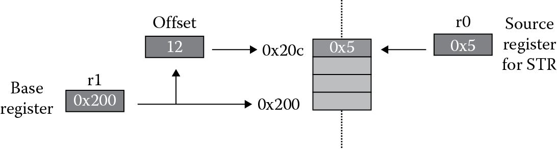
STR r0, [r1, #12]
where register r0 contains 0x5. The store is done by using the value in register r1, 0x200 in this example, as a base address. The offset 12 is added to this address before the data is stored to memory, so the effective address is 0x20C. An important point here is the base register r1 is not modified after this operation. If the value needs to be updated automatically, then the “!” can be added to the instruction, becoming
STR r0, [r1, #12]!
Referring back to Table 5.3, when performing word and unsigned byte accesses on an ARM7TDMI, the offset can be a register shifted by any 5-bit constant, or it can be an unshifted 12-bit constant. For halfword, signed halfword, and signed byte accesses, the offset can be an unsigned 8-bit immediate value or an unshifted register. Offset addressing can use the barrel shifter, which we’ll see in Chapters 6 and 7, to provide logical and arithmetic shifts of constants. For example, you can use a rotation (ROR) and logical shift to the left (LSL) on values in registers before using them. In addition, you can either add or subtract the offset from the base register. As you are writing code, limitations on immediate values and constant sizes will be flagged by the assembler, and if an error occurs, just find another way to calculate your offsets and effective addresses.
Further examples of pre-indexed addressing modes for the ARM7TDMI are as follows:
STR r3, [r0, r5, LSL #3] ; store r3 to ea < r0 + (r5<<3)> (r0 unchanged)
LDR r6, [r0, r1, ROR #6]! ; load r6 from ea < r0 + (r1 >>6)> (r0 updated)
LDR r0, [r1, #-8] ; load r0 from ea < r1-8 >
LDR r0, [r1, -r2, LSL #2] ; load r0 from ea < r1 + (-r2<<2) >
LDRSH r5, [r9] ; load signed halfword from ea < r9 >
LDRSB r3, [r8, #3] ; load signed byte from ea < r8 + 3 >
LDRSB r4, [r10, #0xc1] ; load signed byte from ea < r10 + 193 >
Referring back to Table 5.4, the Cortex-M4 has slightly more restrictive usage. For example, you cannot use a negated register as an offset, nor can you perform any type of shift on a register other than a logical shift left (LSL), and even then, the shift count must be no greater than 3. Otherwise, the instructions look very similar. Valid examples are
LDRSB r0, [r5, r3, LSL #1]
STR r8, [r0, r2]
LDR r12, [r7, #-4]
5.4.2 Post-Indexed Addressing
The post-indexed form of a load or store instruction is:
LDR|STR{<size>}{<cond>} <Rd>, [<Rn>], <offset>
In post-indexed addressing, the effective address of the data transfer is calculated from the unmodified value in the base register, Rn. The offset is then added to the value in Rn, and the sum is written back to Rn. This type of incrementing is useful in stepping through tables or lists, since the base address is automatically updated for you.
Figure 5.2 shows the instruction
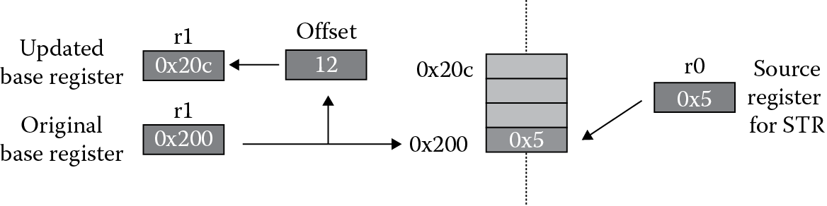
STR r0, [r1], #12
where register r0 contains the value 0x5. In this case, register r1 contains the base address of 0x200, which is used as the effective address. The offset of 12 is added to the base address register after the store operation is complete. Also notice the absence of the “!” option in the mnemonic, since post-indexed addressing always modifies the base register.
As for pre-indexed addressing, the same rules shown in Table 5.3 for ARM7TDMI addressing modes and in Table 5.4 for Cortex-M4 addressing modes apply to post-indexed addressing, too. Examples of post-indexed addressing for both cores include
STR r7, [r0], #24 ; store r7 to ea <r0>, then r0 = r0+24
LDRH r3, [r9], #2 ; load halfword to r3 from ea <r9>, then r9 = r9+2
STRH r2, [r5], #8 ; store halfword from r2 to ea <r5>, then r5 = r5+8
The ARM7TDMI has a bit more flexibility, in that you can even perform rotations on the offset value, such as
LDR r2, [r0], r4, ASR #4; load r2 to ea <r0>, add r4/16 after
Example 5.4
Consider a simple ARM7TDMI program that moves a string of characters from one memory location to another.
SRAM_BASE EQU 0x04000000 ; start of SRAM for STR910FM32
AREA StrCopy, CODE
ENTRY ; mark the first instruction
Main ADR r1, srcstr ; pointer to the first string
LDR r0, =SRAM_BASE ; pointer to the second string
strcopy
LDRB r2, [r1], #1 ; load byte, update address
STRB r2, [r0], #1 ; store byte, update address
CMP r2, #0 ; check for zero terminator
BNE strcopy ; keep going if not
stop B stop ; terminate the program
srcstr DCB “This is my (source) string”, 0
END
The first line of code equates the starting address of SRAM with a constant so that we can just refer to it by name, instead of typing the 32-bit number each time we need it. In addition to the two assembler directives that follow, the program includes two pseudo-instructions, ADR and a special construct of LDR, which we will see in Chapter 6. We can use ADR to load the address of our source string into register r1. Next, the address of our destination is moved into register r0. A loop is then set up that loads a byte from the source string into register r2, increments the address by one byte, then stores the data into a new address, again incrementing the destination address by one. Since the string is null-terminated, the loop continues until it detects the final zero at the end of the string. The BNE instruction uses the result of the comparison against zero and branches back to the label strcopy only if register r2 is not equal to zero. The source string is declared at the end of the code using the DCB directive, with the zero at the end to create a null-terminated string. If you run the example code on an STR910FM32 microcontroller, you will find that the source string has been moved to SRAM starting at address 0x04000000 when the program is finished.
If you follow the suggestions outlined in Appendix A, you can run this exact same code on a Cortex-M4 part, such as the Tiva TM4C123GH6ZRB, accounting for one small difference. On the TI microcontroller, the SRAM region begins at address 0x20000000 rather than 0x04000000. Referring back to the memory map diagram shown in Table 5.1, this region of memory is labeled as bit-banded on-chip SRAM, but for this example, you can safely ignore the idea of a bit-banded region and use it as a simple scratchpad memory. We’ll cover bit-banding in Section 5.6.
5.5 Endianness
The term “endianness” actually comes from a paper written by Danny Cohen (1981) entitled “On Holy Wars and a Plea for Peace.” The raging debate over the ordering of bits and bytes in memory was compared to Jonathan Swift’s satirical novel Gulliver’s Travels, where in the book rival kingdoms warred over which end of an egg was to be broken first, the little end or the big end. Some people find the whole topic more like something out of Alice’s Adventures in Wonderland, where Alice, upon being told by a caterpillar that one side of a perfectly round mushroom would make her grow taller while the other side would make her grow shorter, asks “And now which is which?” While the issue remains a concern for software engineers, ARM actually supports both formats, known as little-endian and big-endian, through software and/or hardware mechanisms.
To illustrate the problem, suppose we had a register that contained the 32-bit value 0x0A0B0C0D, and this value needed to be stored to memory addresses 0x400 to 0x403. Little-endian configurations would dictate that the least significant byte in the register would be stored to the lowest address, and the most significant byte in the register would be stored to the highest address, as shown in Figure 5.3. While it was only briefly mentioned earlier, Examples 5.1, 5.2, and 5.3 are all assumed to be little-endian (have a look at them again).
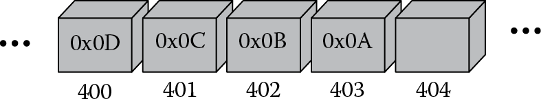
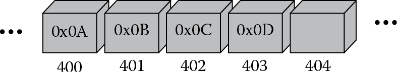
There is really no reason that the bytes couldn’t be stored the other way around, namely having the lowest byte in the register stored at the highest address and the highest byte stored at the lowest address, as shown in Figure 5.4. This is known as word-invariant big-endian addressing in the ARM literature. Using an ARM7TDMI, if you are always reading and writing word-length values, the issue really doesn’t arise at all. You only see a problem when halfwords and bytes are being transferred, since there is a difference in the data that is returned. As an example, suppose you transferred the value 0xBABEFACE to address 0x400 in a little-endian configuration. If you were to load a halfword into register r3 from address 0x402, the register would contain 0x0000BABE when the instruction completed. If it were a big-endian configuration, the value in register r3 would be 0x0000FACE.
ARM has no preference for which you use, and it will ultimately be up to the hardware designers to determine how the memory system is configured. The default format is little-endian, but this can be changed on the ARM7TDMI by using the BIGEND pin. Nearly all microcontrollers based on the Cortex-M4 are configured as little-endian, but more detailed information on byte-invariant big-endian formatting should be reviewed in the Architectural Reference Manual (ARM 2007c) and (Yiu 2014), in light of the fact that word-invariant big-endian format has been deprecated in the newest ARM processors. Many large companies have used a particular format for historical reasons, but there are some applications that benefit from one orientation over another, e.g., reading network traffic is simpler when using a big-endian configuration. All of the coding examples in the book assume a little-endian memory configuration.
For programmers who may have seen memory ordered in a big-endian configuration, or for those who are unfamiliar with endianness, a glimpse at memory might be a little confusing. For example, in Figure 5.5, which shows the Keil development tools, the instruction
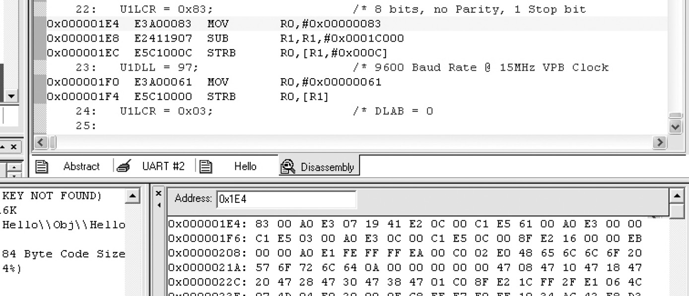
MOV r0, #0x83
can be seen in both the disassembly and memory windows. However, the bit pattern for the instruction is 0xE3A00083, but it appears to be backwards starting at 0x1E4 in the memory window, only because the lowest byte (0x83) has been stored at the lowest address. This is actually quite correct—the disassembly window has taken some liberties here in reordering the data for easier viewing. Code Composer Studio does something similar, so check your tools with a simple test case if you are uncertain. While big-endian addressing might be a little easier to read in a memory window such as this, little-endian addressing can also be easy to read with some practice, and some tools even allow data to be formatted by selecting your preferences.
5.5.1 Changing Endianness
Should it be necessary to swap the endianness of a particular register or a large number or words, the following code can be used for the ARM7TDMI. This method is best for single words.
; On entry: r0 holds the word to be swapped
; On exit : r0 holds the swapped word, r1 is destroyed
byteswap ; r0 = A, B, C, D
EOR r1, r0, r0, ROR #16 ; r1 = A∧C,B∧D,C∧A,D∧B
BIC r1, r1, #0xFF0000 ; r1 = A∧C, 0, C∧A,D∧B
MOV r0, r0, ROR #8 ; r0 = D, A, B, C
EOR r0, r0, r1, LSR #8 ; r0 = D, C, B, A
The following method is best for swapping the endianness of a large number of words:
; On entry: r0 holds the word to be swapped
; On exit : r0 holds the swapped word,
; : r1, r2 and r3 are destroyed
byteswap ; three instruction initialization
MOV r2, #0xFF ; r2 = 0xFF
ORR r2, r2, #0xFF0000 ; r2 = 0x00FF00FF
MOV r3, r2, LSL #8 ; r3 = 0xFF00FF00
; repeat the following code for each word to swap
; r0 = A B C D
AND r1, r2, r0, ROR #24 ; r1 = 0 C 0 A
AND r0, r3, r0, ROR #8 ; r0 = D 0 B 0
ORR r0, r0, r1 ; r0 = D C B A
We haven’t come across the BIC, ORR, or EOR instructions yet. BIC is used to clear bits in a register, ORR is a logical OR operation, and EOR is a logical exclusive OR operation. All will be covered in more detail in Chapter 7, or you can read more about them in the Architectural Reference Manual (ARM 2007c).
After the release of the ARM10 processor, new instructions were added to specifically change the order of bytes and bits in a register, so the v7-M instruction set supports operations such as REV, which reverses the byte order of a register, and RBIT, which reverses the bit order of a register. The example code above for the ARM7TDMI can be done in just one line on the Cortex-M4:
byteswap ; r0 = A B C D
REV r1, r0 ; r1 = D C B A
5.5.2 Defining Memory Areas
The algorithm has been defined, the microcontroller has been identified, the features are laid out for you, and now it’s time to code. When you write your first routines, it will probably be necessary to initialize some memory areas and define variables, and while this is seen again in Chapter 12, it’s probably worth elaborating a bit more here. There are some easy ways to set up tables and constants in your program, and the methods you use depend on how readable you want the code to be. For example, if a table of coefficients is needed, and each coefficient is represented in 8 bits, then you might declare an area of memory as
table DCB 0xFE, 0xF9, 0x12, 0x34
DCB 0x11, 0x22, 0x33, 0x44
if you are reading each value with a LDRB instruction. Assuming that the table was started in memory at address 0x4000 (the compilation tools would normally determine the starting address, but it’s possible to do it yourself), the memory would look like
|
Address |
Data Value |
|
0x4000 |
0xFE |
|
0x4001 |
0xF9 |
|
0x4002 |
0x12 |
|
0x4003 |
0x34 |
|
0x4004 |
0x11 |
|
0x4005 |
0x22 |
|
0x4006 |
0x33 |
|
0x4007 |
0x44 |
If all of the data used will be word-length values, then you’d probably declare an area in memory as
table DCD 0xFEF91234
DCD 0x11223344
but notice that its memory listing in a little-endian system would look like
|
Address |
Data Value |
|
0x4000 |
0x34 |
|
0x4001 |
0x12 |
|
0x4002 |
0xF9 |
|
0x4003 |
0xFE |
|
0x4004 |
0x44 |
|
0x4005 |
0x33 |
|
0x4006 |
0x22 |
|
0x4007 |
0x11 |
In other words, the directives used and the endianness of the system will determine how the data is ordered in memory, so be careful. Since you normally don’t switch endianness while the processor is running, once a configuration is chosen, just be aware of the way the data is stored.
5.6 Bit-Banded Memory
With the introduction of the Cortex-M3 and M4 processors, ARM gave programmers the ability to address single bits more efficiently. Imagine that some code wants to access only one particular bit in a memory location, say bit 2 of a 32-bit value held at address 0x40040000. Microcontrollers often use memory-mapped registers in place of registers in the core, especially in industrial microcontrollers where you have ten or twenty peripherals, each with its own set of unique registers. Let’s further say that a peripheral such as a Controller Area Network (CAN) controller on the Tiva TM4C123GH6ZRB, which starts at memory address 0x40040000, has individual control bits that are set or cleared to enable different modes, read status information, or transmit data. For example, bit 7 of the CAN Control Register puts the CAN controller in test mode. If we wish to set this bit and only this bit, you could use a read-modify-write operation such as:
LDR r3, =0x40040000 ; location of CAN Control Register
LDR r2, [r3] ; read the memory-mapped register contents
ORR r2, #0x80 ; set bit 7
STR r2, [r3] ; write the entire register contents back
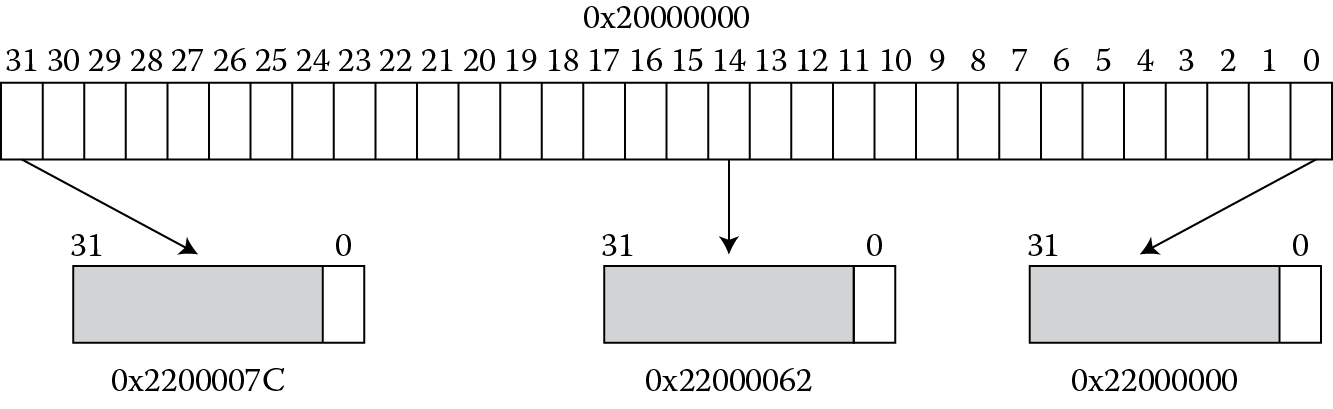
This seems horribly wasteful from a code size and execution time perspective to set just one bit in a memory-mapped register. Imagine then if every bit in a register had its own address—rather than loading an entire register, modifying one bit, then writing it back, an individual bit could be set by just writing to its address. Examining Table 5.1 again, you can see that there are two bit-banded regions of memory: addresses from 0x22000000 to 0x220FFFFF are used specifically for bit-banding the 32KB region from 0x20000000 to 0x20007FFF; and addresses from 0x42000000 to 0x43FFFFFF are used specifically for bit-banding the 1MB region from 0x40000000 to 0x400FFFFF. Figure 5.6 shows the mapping between the regions. Going back to the earlier CAN example, we could set bit 7 using just a single store operation:
LDR r3, =0x4280001C
MOV r4, #1
STR r4, [r3] ; set bit 7 of the CAN Control Register
The address 0x4280001C is derived from
bit-band alias = bit-band base + (byte offset × 32) + (bit number × 4)
= 0x42000000 + (0x40000 × 0x20) + (7 × 4)
= 0x42000000 + 0x800000 + 0x1C
As another example, if bit 1 at address 0x40038000 (the ADC 0 peripheral) is to be modified, the bit-band alias is calculated as:
0x42000000 + (0x38000 × 0x20) + (1 × 4) = 0x42700004
What immediately becomes obvious is that you would need a considerable number of addresses to make a one-to-one mapping of addresses to individual bits. In fact, if you do the math, to have each bit in a 32KB section of memory given its own address, with each address falling on a word boundary, i.e., ending in either 0, 4, 8, or C, you would need
32,768 bytes × 8 bits/byte × 4 bytes/bit = 1MB
The trade-off then becomes an issue of how much address space can be sacrificed to support this feature, but given that microcontrollers never use all 4GB of their address space, and that large swaths of the memory map currently go unused, this is possible. Perhaps in ten years, it might not be.
5.7 Memory Considerations
In a typical microcontroller, there are often blocks of volatile memory (SRAM or some other type of RAM) available for you to use, along with different kinds of non-volatile memory (flash or ROM) where your code would live. Simulators such as Keil’s RealView Microcontroller Development Kit model those different blocks of memory for you, so you don’t necessarily stop to think about how code was loaded into flash or how some variables ended up in SRAM. As a programmer, you write your code, press a few buttons, and voilà—things just work. Describing what happens behind the scenes and all the options associated with emulation and debugging could easy fill another book, but let’s at least see how blocks of memory are configured as we declare sections of code.
Consider a directive used in a program to reserve some space for a stack (a stack is a section of memory used during exception processing and subroutines which we’ll see in Chapters 13, 14 and 15, but for now we are just telling the processor to reserve a section of RAM for us). Our directive might look like
AREA STACK, NOINIT, READWRITE, ALIGN = 3
StackMem
SPACE Stack
If we are programming something like a microcontroller, then we also have our program that needs to be stored in flash memory, so that when the processor is reset, code already exists in memory to be executed. The start of our program might look like
AREA RESET, CODE, READONLY
THUMB
;************************************************************
;
; The vector table.
;
;************************************************************
DCD StackMem + Stack ;Top of Stack
DCD Reset_Handler ; Reset Handler
DCD NmiSR ; NMI Handler
DCD FaultISR ; Hard Fault Handler
.
.
.
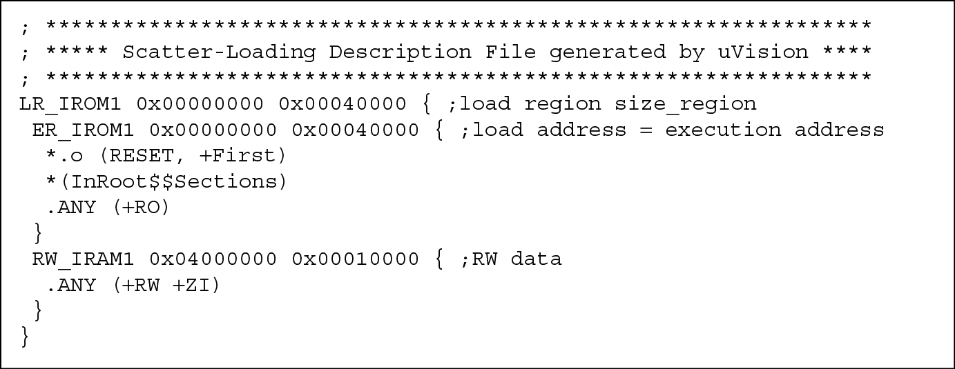
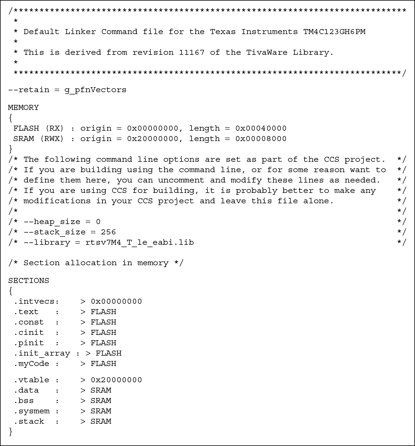
At this point, something is missing—how does a development tool know that there is a block of RAM on our microcontroller for things like stacks, and how does it know the starting address of that block? When you first start your simulation, you likely pick a part from a list of available microcontrollers (if you use the Keil tools), and the map of the memory system is already configured in the tool for you. When you assemble your program, the tools will generate a map file such as the one in Figure 5.7 (Keil) or Figure 5.8 (CCS) which shows where code and variables are actually stored. The linker then uses this information when building an executable to ensure the various sections (in the object files created by the assembler) are placed in the appropriate memories, where sections are built with the AREA directives we have been using. In Figure 5.7, you can see that the section that we called RESET, which is our program, would be stored to ROM starting at address 0x0. Any read-only sections are also stored to this ROM region. Read/write and zero-initialized data would be stored to RAM starting at address 0x04000000, which is where the SRAM block is located on an STR910FM32 microcontroller, in this example. You can also create your own custom scatter-loading file to feed into the linker, and those details can be found in RealView Compilation Tools Developer Guide (ARM 2007a).
Other techniques, like those used in the gnu tools, can be used to assign variables to certain regions of memory. For example, in C, it is possible to tell the linker to place a variable at a specific location in memory. If you were writing code, you might say something like:
#include <stdio.h >
extern int cube(int n1);
int gCubed __attribute__((at(0x9000))); // Place at 0x9000
int main()
{
gCubed = cube(3);
printf(“Your number cubed is: %d\n”, gCubed);
}
Your global variable called gCubed would be placed at the absolute address 0x9000. In most instances, it is still far easier to control variables and data using directives.
5.8 Exercises
- Describe the contents of register r13 after the following instructions complete, assuming that memory contains the values shown below. Register r0 contains 0x24, and the memory system is little-endian.
Address
Contents
0x24
0x06
0x25
0xFC
0x26
0x03
0x27
0xFF
- LDRSB r13, [r0]
- LDRSH r13, [r0]
- LDR r13, [r0]
- LDRB r13, [r0]
- Indicate whether the following instructions use pre- or post-indexed addressing modes:
- STR r6, [r4, #4]
- LDR r3, [r12], #6
- LDRB r4, [r3, r2]!
- LDRSH r12, [r6]
- Calculate the effective address of the following instructions if register r3 = 0x4000 and register r4 = 0x20:
- STRH r9, [r3, r4]
- LDRB r8, [r3, r4, LSL #3]
- LDR r7, [r3], r4
- STRB r6, [r3], r4, ASR #2
- What’s wrong with the following instruction running on an ARM7TDMI?
- LDRSB r1,[r6],r3,LSL#4
- Write a program for either the ARM7TDMI or the Cortex-M4 that sums word-length values in memory, storing the result in register r3. Include the following table of values to sum in your code:
TABLE DCD 0xFEBBAAAA, 0x12340000, 0x88881111
DCD 0x00000013, 0x80808080, 0xFFFF0000
- Assume an array contains 30 words of data. A compiler associates variables x and y with registers r0 and r1, respectively. Assume the starting address of the array is contained in register r2. Translate the C statement below into assembly instructions:
- x = array[7] + y;
- Using the same initial conditions as Exercise 6, translate the following C statement into assembly instructions:
- array[10] = array[8] + y;
- Consider a C procedure that initializes an array of bytes to all zeros, given as
init_Indices (int a[], int s) {int i;
for (i = 0; i < s; i++)
a[i] = 0;}
- Write the assembly language for this initialization routine. Assume s > 0 and is held in register r2. Register r1 contains the starting address of the array, and the variable i is held in register r3. While loops are not covered until Chapter 8, you can build a simple for loop using the following construction:
MOV r3, #0 ; clear i
loop instructioninstructionADD r3, r3, #1 ; increment i
CMP r3, r2 ; compare i to s
BNE loop ; branch to loop if not equal
- Suppose that registers belonging to a particular peripheral on a microcontroller have a starting address of 0xE000C000. Individual registers within the peripheral are addressed as offsets from the starting address. If a register called LSR0 is 0x14 bytes away from the starting address, write the assembly and Keil directives that will load a byte of data into register r6, where the data is located in the LSR0 register. Use pre-indexed addressing.
- Assume register r3 contains 0x8000. What would the register contain after executing the following instructions?
- STR r6, [r3, #12]
- STRB r7, [r3], #4
- LDRH r5, [r3], #8
- LDR r12, [r3, #12]!
- Assuming you have a little-endian memory system connected to the ARM7TDMI, what would register r4 contain after executing the following instructions? Register r6 holds the value 0xBEEFFACE and register r3 holds 0x8000.
STR r6, [r3]
LDRB r4, [r3]
- What if you had a big-endian memory system?
* The term megabyte is used loosely these days, as 1 kilobyte is defined as 210 or 1024 bytes. A megabyte is 220 or 1,048,576 bytes, but it is abbreviated as 1 million bytes. The distinction is rarely important.