Table of Contents for
ARM Assembly Language, 2nd Edition
 ARM Assembly Language, 2nd Edition
Published by
Chapman and Hall/CRC, 2016
ARM Assembly Language, 2nd Edition
Published by
Chapman and Hall/CRC, 2016
- Contents
- ARM Assembly Language: Fundamentals and Techniques, Second Edition
- Preliminaries
- To our families
- Preface
- Acknowledgments
- Authors
- Chapter 1 - An Overview of Computing Systems
- Chapter 2 - The Programmer’s Model
- Chapter 3 - Introduction to Instruction Sets: v4T and v7-M
- Chapter 4 - Assembler Rules and Directives
- Chapter 5 - Loads, Stores, and Addressing
- Chapter 6 - Constants and Literal Pools
- Chapter 7 - Integer Logic and Arithmetic
- Chapter 8 - Branches and Loops
- Chapter 9 - Introduction to Floating-Point: Basics, Data Types, and Data Transfer
- Chapter 10 - Introduction to Floating-Point: Rounding and Exceptions
- Chapter 11 - Floating-Point Data-Processing Instructions
- Chapter 12 - Tables
- Chapter 13 - Subroutines and Stacks
- Chapter 14 - Exception Handling: ARM7TDMI
- Chapter 15 - Exception Handling: v7-M
- Chapter 16 - Memory-Mapped Peripherals
- Chapter 17 - ARM, Thumb and Thumb-2 Instructions
- Chapter 18 - Mixing C and Assembly
- Appendix A: Running Code Composer Studio
- Appendix B: Running Keil Tools
- Appendix C: ASCII Character Codes
- Appendix D
- Glossary
- References
Chapter 7
Integer Logic and Arithmetic
7.1 Introduction
This is a long chapter, but for good reasons. Arithmetic operations are probably one of the more common types of instructions you will use, especially if the software being written involves manipulating large amounts of data, such as an incoming audio signal. Graphics algorithms, speech processing algorithms, digital controllers, and audio processing all involve a great deal of arithmetic work, so it’s important to understand the types of data that you have and how to perform the operation needed in the shortest amount of time and/or space. We begin with a discussion of flags, examine the basic arithmetic instructions for both the ARM7TDMI and the Cortex-M4, quickly examine some of the new DSP extensions in the Cortex-M4, and then wrap up with an overview of fractional arithmetic. Once you gain a good understanding of the concepts behind integer arithmetic, you should then be able to tackle floating-point arithmetic in Chapters 9, 10, and 11, and even go on to more advanced functions, such as trigonometric functions, exponentials, and square roots.
7.2 Flags and Their Use
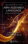
Recall from Chapter 2 that the Program Status Register holds the current state of the machine: the flags, the mode, the interrupt bits, and the Thumb bit for the ARM7TDMI, and the flags, the exception number, the Interrupt-Continuable Instruction (ICI) bits, and the Thumb bit for the Cortex-M4, shown in Figure 7.1. There are four bits, N, Z, C, and V, in the uppermost nibble that help determine whether or not an instruction will be conditionally executed. The flags are set and cleared based on one of four things:
- Instructions that are specifically used for setting and clearing flags, such TST or CMP
- Instructions that are told to set the flags by appending an “S” to the mnemonic. For example, EORS would perform an exclusive OR operation and set the flags afterward, since the S bit is set in the instruction. We can do this with all of the ALU instructions, so we control whether or not to update the flags
- A direct write to the Program Status Register, where you explicitly set or clear flags
- A 16-bit Thumb ALU instruction, which will be covered both here and in Chapter 17
The Q flag on the Cortex-M4 indicates a value has saturated and different rules govern its behavior, so it is discussed separately in Section 7.4.4. In the next sections, we’ll examine each flag individually—some are quite easy and some require a little thought.
7.2.1 The N Flag
This flag is useful when checking for a negative result. What does this mean, negative? This definition sits in the context of a two’s complement number system, and as we saw in the last few chapters, a two’s complement number is considered to be negative if the most significant bit is set. Be careful, though, as you could easily have two perfectly good positive numbers add together to produce a value with the uppermost bit set.
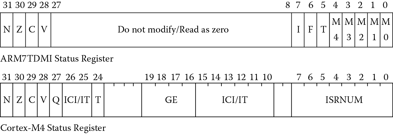
Example 7.1
Adding −1 to −2 is easy enough, and the result has the most-significant bit set, as expected. In two’s complement notation, this would be represented as
If we were to code this on the ARM7TDMI as
MOV r3, #-1
MOV r4, #-2
ADDS r3, r4, r3
we would expect to see the N bit set in the CPSR, as shown in Figure 7.2, which it is, as the most significant bit of register r3 was set as a result of the addition.
Example 7.2
If we add the values below, the addends are positive in two’s complement notation, but the sum is negative, i.e.,
which means that something might be wrong. First, notice that since the most-significant bit is now set, this forces the N bit to be set if our ADD instruction actually sets the flags (remember, it doesn’t have to). Second, if you aren’t working with two’s complement numbers, then perhaps we don’t really care what the value of the N bit is. Finally, in a two’s complement representation, notice that we originally meant to add two positive numbers together to get a bigger positive sum, but the result indicates that this positive sum cannot be represented in 32 bits, so the result effectively overflowed the precision we had available. So perhaps we need one more flag to work with signed values.
7.2.2 The V Flag
When performing an operation like addition or subtraction, if we calculate the V flag as an exclusive OR of the carry bit going into the most significant bit of the result with the carry bit coming out of the most significant bit, then the V flag accurately indicates a signed overflow. Overflow occurs if the result of an add, subtract, or compare is greater than or equal to 231, or less than –231.
Example 7.3
Two signed values, assumed to be in two’s complement representations, are added to produce the sum
which does not fit into 32 bits. More importantly, since the numbers are considered to be in a two’s complement format, then we overflowed, since we added two fairly large, negative numbers together, and the most significant bit of the 32-bit result is clear (notice the 5 in the most significant byte of the result).
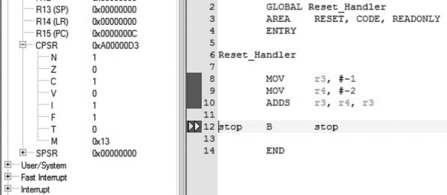
Let’s examine Example 7.2 again. When we added 0x7B000000 to 0x30000000, the result did, in fact, fit into 32 bits. However, the result would be interpreted as a negative number when we started off adding two positive numbers, so is this an overflow case? The answer is yes. Both the N and the V bits would be set in the xPSR, as shown in Figure 7.3, if you were to run the following code on the Cortex-M4:
LDR r3, =0x7B000000
LDR r4, =0x30000000
ADDS r5, r4, r3
Notice that the ‘S’ extension is added to the ADD mnemonic, indicating that we want the flags updated as a result of the addition.
7.2.3 The Z Flag
This is one of the easiest to understand, as the only thing the Z flag tells us is that the result of an operation produces zero, meaning all 32 bits must be zero. This might be the result of a counter expiring, or a routine might need to examine an operand before performing some other kind of arithmetic routine, such as division.
Example 7.4
In Chapter 16, we’ll create a short program to change the color of the LED on the Tiva Launchpad, part of which is shown below.
MOVT r7, #0xF4 ; set counter to 0xF40000
spin
SUBS r7, r7, #1 ; just twiddling our thumbs....
BNE spin
In order to hold the LED at a particular color for a second or two, a short loop sets a register to a fixed value then subtracts one, setting the flags in the process, until the register equals zero. The Z flag is used to determine when the counter hits zero, where the BNE (branch if not equal to zero) instruction uses the value of the Z flag. If it is clear, then the program jumps back to the SUBS instruction and repeats. Otherwise, the loop is exhausted and the program continues doing something else.
7.2.4 The C Flag
The Carry flag is set if the result of an addition is greater than or equal to 232, if the result of a subtraction is positive, or as the result of an inline barrel shifter operation in a move or logical instruction. Carry is a useful flag, allowing us to build operations with greater precision should we need it, e.g., creating routines to add 64-bit numbers, which we will see in a moment. If we were to add the two values shown in the code below, the C bit will be set in the status register, since the sum is greater than 232.
LDR r3, =0x7B000000
LDR r7, =0xF0000000
ADDS r4, r7, r3 ; value exceeds 32 bits, generates C out
Like older processors, such as the MC68000 and its predecessors, the carry flag is inverted after a subtraction operation, making the carry bit more like a borrow bit, primarily due to the way subtraction is implemented in hardware. For example, these instructions will set the carry bit to a one, since the operation produces no carry out and the bit is inverted:
LDR r0, =0xC0000000
LDR r2, =0x80000000
SUBS r4, r0, r2 ; r4 = r0 - r2 (watch the order!)
Let’s further suppose that we really want to subtract two 64-bit numbers:
0x7000BEEFC0000000
− 0x3000BABE80000000
We know the answer should be 0x4000043140000000, and to get this, we use the following code:
LDR r0, =0xC0000000 ; lower 32-bits
LDR r1, =0x7000BEEF ; upper 32-bits
LDR r2, =0x80000000 ; lower 32-bits
LDR r3, =0x3000BABE ; upper 32-bits
SUBS r4, r0, r2 ; set C bit for next subtraction
SBC r5, r1, r3 ; upper 32 bits use the carry flag
The first subtraction operation will set the status flags for us. We saw earlier that the C flag is set, since there is no carry out for the first operation, e.g., 0xC minus 0x8 produces no carry. The second subtraction is a subtract with carry (SBC) operation, using the carry bit to perform a normal subtraction. If the carry bit had been clear, the SBC instruction would have subtracted one more from its result.
7.3 Comparison Instructions
Apart from using the S bit with instructions to set flags, there are also four instructions that do nothing except set the condition codes or test for a particular bit in a register. They are:
CMP—Compare. CMP subtracts a register or an immediate value from a register value and updates the condition codes. You can use CMP to quickly check the contents of a register for a particular value, such as at the beginning or end of a loop.
CMN—Compare negative. CMN adds a register or an immediate value to another register and updates the condition codes. CMN can also quickly check register contents. This instruction is actually the inverse of CMP, and the assembler will replace a CMP instruction when appropriate. For example, if you typed
CMP r0, #-20
the assembler will instead generate
CMN r0, #0x14
TST—Test. TST logically ANDs an arithmetic value with a register value and updates the condition codes without affecting the V flag. You can use TST to determine if many bits of a register are all clear or if at least one bit of a register is set.
TEQ—Test equivalence. TEQ logically exclusive ORs an arithmetic value with a register value and updates the condition codes without affecting the V flag. You can use TEQ to determine if two values are the same.
The syntax for these instructions is
instruction{<cond>} <Rn>, <operand2>
where {<cond>} is one of the optional conditions covered in Chapter 8, and <operand2> can be a register with an optional shift, or an immediate value. Typical instructions might look like
CMP r8, #0 ; r8 = =0?
BEQ routine ; yes, then go to my routine
TST r4, r3 ; r3 = 0xC0000000 to test bits 31, 30
TEQ r9, r4, LSL #3
Recall that the condition code flags are kept in the Program Status Register, along with other state information, such as the mode (for the ARM7TDMI) or the current exception number (for the Cortex-M4). For both processors, you can use the MRS (Move PSR to general-purpose register) instruction to read the flags, and the MSR (Move general-purpose register to PSR) to write the flags.
The ARM7TDMI has both Current and Saved Program Status Registers, so the MRS instruction will read the flags in the CPSR and any of the SPSRs. For example, the two instructions
MRS r0, CPSR
MRS r1, SPSR
will load the contents of the CPSR and SPSR into registers r0 and r1, respectively. From there, you can examine any flags that you like. The restrictions here are that you cannot use register r15 as the destination register, and you must not attempt to access an SPSR in User mode, since the register does not exist. The ARM Architectural Reference Manual (ARM 2007c) defines the results of this operation as UNPREDICTABLE.
The Cortex-M4 has only one status register, but it can be referenced in three different views—APSR, IPSR, or EPSR—or all at once as PSR. The flags are held only in the APSR, so you could read or change the values using
MRS r3, APSR ; read flag information into r3
MSR APSR, r2 ; write to just the flags
MSR PSR, r7 ; write all status information to r7
As we begin to write more complex programs, individual flags will become less important, and you will more than likely use the condition codes along with a branch (B) instruction or another instruction to create loops and conditional assembly routines without actually having to read the flags, for example, the BEQ instruction above. This topic is covered in much more detail in Chapter 8.
7.4 Data Processing Operations
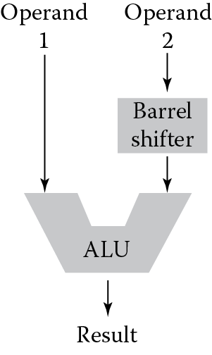
You would expect any microprocessor, even the simplest, to include the fundamental operations such as add, subtract, and shift, and from these you could build more advanced operations such as divide, multiply, and square root. The ARM microprocessors are designed to be used in embedded applications, which are very sensitive to power dissipation and die size. Ideally, the processor would provide a wide range of data processing instructions without making the gate count of the part too high or make the area requirements too large. By combining a barrel shifter, a 32-bit ALU, and a hardware multiplier, the ARM7TDMI provides a rich instruction set while saving power. With significant advances in CMOS processes, more transistors can be used in VLSI designs the size of the ARM7TDMI or smaller, allowing for even more arithmetic functionality to be added to the Cortex-M4, such as a hardware divider, saturated math and DSP operations, and even a floating-point unit!
An example of a data processing instruction, ADD, might look like
ADDS{<cond>} r0, r1, <operand2>
where “S” indicates that the status flags should be updated and {<cond>} is one of the optional conditions covered in Chapter 8, e.g., EQ, LT, GT, or PL. The second operand, <operand2>, can be an immediate value, a register, or a register with a shift or rotate associated with it. The last option turns out to be quite handy, as we’ll see below. As an aside, this syntax has been updated for Unified Assembly Language (UAL)—the older style of mnemonic would have been written as ADD{<cond>}S,* and we will see how even shifts and rotations have changed their format.
7.4.1 Boolean Operations
Both the ARM7TDMI and the Cortex-M4 support Boolean logic operations using two register operands, shown in Table 7.1. Although we saw MOV instructions in previous chapters, the MOVN instruction can also be used to logically invert all bits in a register, since it takes the one’s complement negation of an operand. A very fast way to load the two’s complement representation of −1 into a register is to logically invert zero, since the 32-bit value 0xFFFFFFFF is −1 in a two’s complement notation, written as
Boolean Operations
|
ARM7TDMI Instruction |
Cortex-M4 Instruction |
Comment |
|
AND |
AND |
Logically ANDs two operands |
|
ORR |
ORR |
Logically ORs two operands |
|
ORN |
OR of operand 1 with NOT operand 2 |
|
|
EOR |
EOR |
Exclusive OR of two operands |
|
MOVN |
MVN |
Move negative—logically NOTs all bits |
|
BIC |
BIC |
Bit Clear—clears selected bits in a register |
MOVN r5, #0 ; r5 = −1 in two’s complement
Examples of the remaining operations include
AND r1, r2, r3 ; r1 = r2 AND r3
ORR r1, r2, r3 ; r1 = r2 OR r3
EOR r1, r2, r3 ; r1 = r2 exclusive OR r3
BIC r1, r2, r3 ; r1 = r2 AND NOT r3
The first three instructions are fairly straightforward—AND, OR, and exclusive OR are basic logic functions. The fourth instruction is the Bit Clear operation, which can be used to clear selected bits in a register. For each bit in the second operand, a 1 clears the corresponding bit in the first operand (a register), and a 0 leaves it unchanged. According to the data processing instruction format, we can also use an immediate value for the second operand. For example,
BIC r2, r3, #0xFF000000
clears the upper byte of register r3 and moves the result to register r2.
The Cortex-M4 has one additional Boolean operation called ORN, for OR Not, which logically ORs the first operand with the one’s complement of the second operand.
7.4.2 Shifts and Rotates
Figure 7.4 shows part of the internal data path of the ARM7TDMI, where the data for an instruction come down two busses leading to the main ALU. Only one of those busses goes through the barrel shifter, which is a dedicated hardware block of logic to rotate or shift data left or right. Because of this asymmetry, we can rotate or shift only one of the operands in the instruction, but in general, this is enough functionality. With the addition of a few instructions, we can overcome any limitations that are introduced with this type of design. In fact, the very idea to have a barrel shifter sit between the register bank (an architecture term that describes the physical registers r0 through r15) and the main ALU allows for 32-bit constants to be used in ALU and MOV instructions, despite having only 32 bits for the instruction itself. We saw this in Chapter 6 with literals and constants.
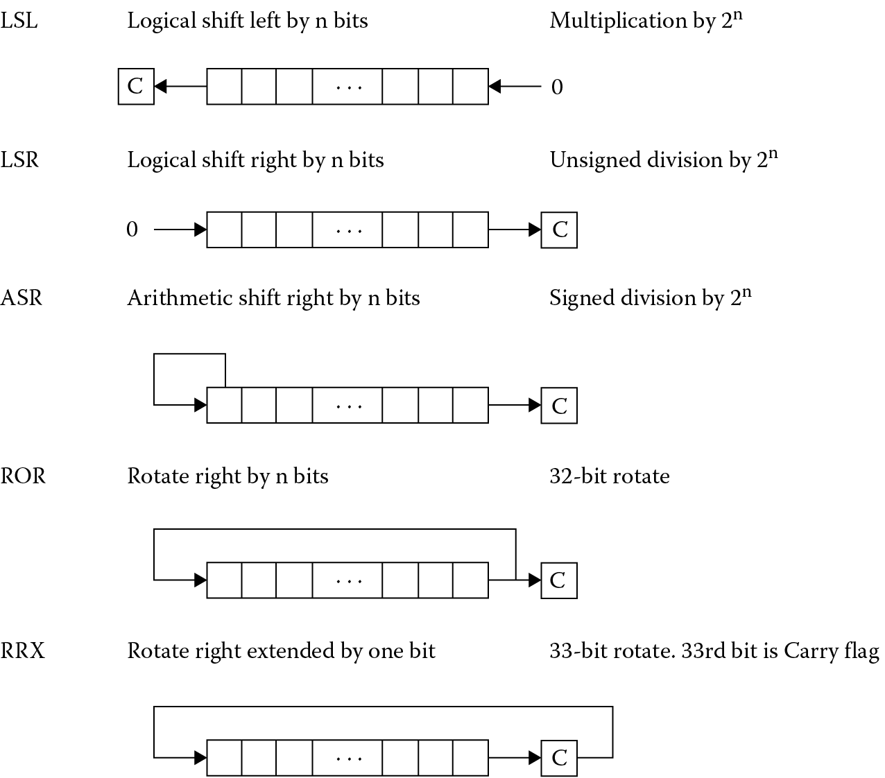
The types of shifts and rotates that the ARM processors can perform are shown in Figure 7.5. There are two types of logical shifts, where the data is treated as unsigned, an arithmetic shift where the data is treated as signed, and two types of rotates. The absence of rotate left can be explained by the fact that a rotate left by m bits is the same as a rotate to the right by (32-m) bits (except for the effect on the carry bit), and can, therefore, be done using the same instruction. Another instruction that may appear to have gone missing is ASL, or an arithmetic shift left. With a little thought, it becomes apparent that you would never need such an instruction, since arithmetic shifts need to preserve the sign bit, and shifting signed data to the left will do so as long as the number doesn’t overflow. As an example, the number −1 in two’s complement notation is 0xFFFFFFFF, and shifting it left results in 0xFFFFFFFE, which is −2 and correct. A 32-bit number such as 0x8000ABCD will overflow if shifted left, resulting in 0x0001579A, which is now a positive number.
If you want to shift or rotate data without performing another operation such as an add, then a MOV instruction works well. Recall from Chapter 6 that MOV can transfer data from a register to a register, so by adding an optional shift operation, the instruction gets slightly more elaborate. When you follow the UAL conventions, an instruction that just shifts data to the left should use the LSL mnemonic; an instruction that just shifts data to the right should use the LSR mnemonic. The assembler will choose the best instruction to use under the guidelines of the assembly directives that are given. For example, code that is written as
LSL r3, r4, #1
for an ARM7TDMI will be replaced with
MOV r3, r4, LSL #1
assuming that you have not explicitly told the assembler you want Thumb instructions. On a Cortex-M4, the assembler will replace this with the 32-bit Thumb-2 instruction
LSL r3, r4, #1
because the original mnemonic does not set the flags, and neither will the 32-bit version. Thumb arithmetic instructions set flags automatically, so if you said
LSLS r3, r3, #1
you would get the 16-bit Thumb instruction
LSL r3, #1
More will be said about Thumb in Chapter 17.
Example 7.5
The following instructions show how simple shifts and rotates are written.
LSL r4, r6, #4 ; r4 = r6 << 4 bits
LSL r4, r6, r3 ; r4 = r6 << # specified in r3
ROR r4, r6, #12 ; r4 = r6 rotated right 12 bits
; r4 = r6 rotated left 20 bits
All shift operations take one clock cycle to execute, except register-specified shifts, which take an extra cycle as there are only two read ports on the register bank, and an extra read is required. When performing shifts, the shift count can be either an unsigned 5-bit value, i.e., 0 to 31, as in the first example, or the bottom byte in a register, as in the second example.
Example 7.6
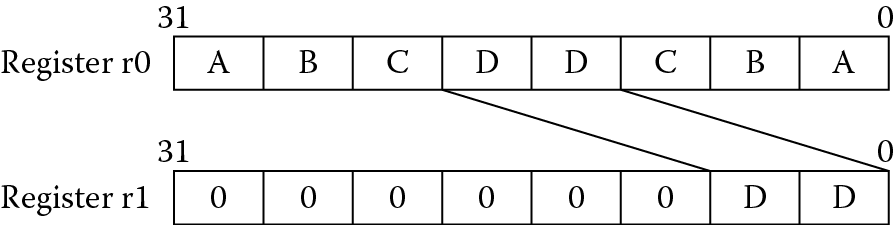
The shift and logical operations can also be used to move data from one byte to another. Suppose we need to move the uppermost byte from register r2 and put it at the bottom of register r3. The contents of register r3 are shifted left by 8 bits first. Two instructions could be used to do this:
LSR r0, r2, #24 ; extract top byte from R2 into R0
ORR r3, r0, r3, LSL #8 ; shift up r3 and insert r0
Example 7.7 Hamming Codes
In the 1940s, a mathematician named Richard Hamming developed and formally defined ways of not only detecting errors in bit streams but correcting them as well. For example, if you were going to transmit 8 bits of data from a computer across a channel (and here, a channel could be seen as something like a piece of wire, an optical link, or maybe even a wireless interface) to a receiver, you would hope that the value you sent matches the value received exactly. If there are errors, it’s critical to know this. More interestingly, if there is a way to correct the bit error, this byte of information would not need to be resent. The field of error correcting codes has grown substantially since then, and more modern coding schemes such as Reed-Solomon code, Binary Golay code, and BCH code can be found in Roth (2006). While the theory behind them is rather complicated, simple Hamming codes can be built easily, so we’ll examine an algorithm to detect up to two bit errors in an 8-bit value. This algorithm can also correct a single bit error.
Consider the idea of adding a bit, called a checksum, to a value that indicates the parity of the bits in that value. For example, if you had the 7-bit number
1010111
and we counted the number of ones in the value, 5 in this case, adding a 1 at the beginning of the value would make the parity even, since the number of ones (including the parity bit) is an even number. Our new value would be
11010111
If the data were transmitted this way, the receiver could detect an error in the byte sent if one of the data bits changes, since the parity would suddenly become odd. Note that if two of the bits changed, then we could not detect an error, since the parity remains even.
One type of Hamming code can be constructed by using four checksum bits placed in strategic locations. If a 12-bit value is constructed using 8 bits of data and four checksum bits as shown below, then we can use the checksum bits to detect up to two errors in the data and even correct a single bit error.
Original 8-bit value
|
d7 |
d6 |
d5 |
d4 |
d3 |
d2 |
d1 |
d0 |
Modified 8-bit value
|
11 |
10 |
9 |
8 |
7 |
6 |
5 |
4 |
3 |
2 |
1 |
0 |
|
d7 |
d6 |
d5 |
d4 |
c3 |
d3 |
d2 |
d1 |
c2 |
d0 |
c1 |
c0 |
The checksum bits c3, c2, c1, and c0 are computed as follows:
Checksum bit c0 should produce even parity for bits 0, 2, 4, 6, 8, and 10. In other words, we’re checking a bit, skipping a bit, checking a bit, etc.
Checksum bit c1 should produce even parity for bits 1, 2, 5, 6, 9, and 10. In other words, we’re checking two bits, skipping two bits, checking two bits, etc.
Checksum bit c2 should produce even parity for bits 3, 4, 5, 6, and 11. Now we’re checking four bits, skipping four bits, etc.
Checksum bit c3 should produce even parity for bits 7, 8, 9, 10, and 11.
As an example, suppose we wanted to generate checksums for the binary value 10101100. The first checksum bit c0 would be 1, since this would produce even parity for the bits 0, 0, 1, 0, and 0. Using the same method, the remaining checksum bits would show
c1 = 1
c2 = 1
c3 = 0
resulting in the 12-bit value 101001101011.
The code on the next page shows the assembly code to build a 12-bit Hamming code, making efficient use of the barrel shifter during logical operations.
AREA HAMMING, CODE
ENTRY
; Registers used:
; R0 - temp
; R1 - used to hold address of data
; R2 - holds value to be transmitted
; R4 - temp
main
MOV r2, #0 ; clear out transmitting reg
ADR r1, arraya ; start of constants
LDRB r0, [r1]
;
; calculate c0 using bits 76543210
; * ** **
; even parity, so result of XORs is the value of c0
;
MOV r4, r0 ; make a copy
EOR r4, r4, r0, ROR #1 ; 1 XOR 0
EOR r4, r4, r0, ROR #3 ; 3 XOR 1 XOR 0
EOR r4, r4, r0, ROR #4 ; 4 XOR 3 XOR 1 XOR 0
EOR r4, r4, r0, ROR #6 ; 6 XOR 4 XOR 3 XOR 1 XOR 0
AND r2, r4, #1 ; create c0 -> R2
;
; calculate c1 using bits 76543210
; * * ** *
MOV r4, r0
EOR r4, r4, r0, ROR #2 ; 2 XOR 0
EOR r4, r4, r0, ROR #3 ; 3 XOR 2 XOR 0
EOR r4, r4, r0, ROR #5 ; 5 XOR 3 XOR 2 XOR 0
EOR r4, r4, r0, ROR #6 ; 6 XOR 5 XOR 3 XOR 2 XOR 0
AND r4, r4, #1 ; isolate bit
ORR r2, r2, r4, LSL #1 ; 7 6 5 4 3 2 c1 c0
;
; calculate c2 using bits 76543210
; * ***
ROR r4, r0, #1 ; get bit 1
EOR r4, r4, r0, ROR #2 ; 2 XOR 1
EOR r4, r4, r0, ROR #3 ; 3 XOR 2 XOR 1
EOR r4, r4, r0, ROR #7 ; 7 XOR 3 XOR 2 XOR 1
AND r4, r4, #1 ; isolate bit
ORR r2, r2, r4, ROR #29 ; 7 6 5 4 c2 2 c1 c0
;
; calculate c3 using bits 76543210
; ****
ROR r4, r0, #4 ; get bit 4
EOR r4, r4, r0, ROR #5 ; 5 XOR 4
EOR r4, r4, r0, ROR #6 ; 6 XOR 5 XOR 4
EOR r4, r4, r0, ROR #7 ; 7 XOR 6 XOR 5 XOR 4
AND r4, r4, #1
;
; build the final 12-bit result
;
ORR r2, r2, r4, ROR #25 ; rotate left 7 bits
AND r4, r0, #1 ; get bit 0 from original
ORR r2, r2, r4, LSL #2 ; add bit 0 into final
BIC r4, r0, #0xF1 ; get bits 3,2,1
ORR r2, r2, r4, LSL #3 ; add bits 3,2,1 to final
BIC r4, r0, #0x0F ; get upper nibble
ORR r2, r2, r4, LSL #4 ; r2 now contains 12 bits
; with checksums
done B done
ALIGN
arraya
DCB 0xB5
DCB 0xAA
DCB 0x55
DCB 0xAA
END
Our starting 8-bit value is in memory location arraya and is loaded into register r0. A fast way to generate even parity is to use the result of exclusive OR operations as the checksum bit, e.g., if you take an odd number of bits in a pattern and exclusive OR them together, the result will be 1; therefore, the checksum should be a 1 to make an even number. The first checksum is generated by using an EOR instruction on the original data many times, ignoring all bits except bit 0. Note that the first logical instruction
EOR r4, r4, r0, ROR #1
takes the original data and exclusive ORs bit 0 with bit 1 of the copied data, all in a single instruction. Subsequent EOR instructions take the copied data and rotate the necessary bits down to bit 0. Ultimately, we’re only interested in bit 0, so we logically AND the final result with 1 to clear out all the bits except the least significant bit, since ANDing a value with 0 produces 0, and ANDing a value with 1 just gives back the original value.
The other checksums are calculated in much the same way, always shifting the necessary bits down to bit 0 before EORing them with intermediate results. The final 12-bit value is constructed from the original 8-bit value and the four checksums using logical functions. Notice that rotates to the left are done using ROR instructions, since a rotate to the left by n bits is the same as a rotate to the right by (32-n) bits, and there is no ROL instruction. The final value is kept in register r2. The first 8-bit value read, 0xB5, should generate the 12-bit Hamming value 0xBA6 in register r2.
To detect an error in the transmitted value, the four checksum bits c3, c2, c1, and c0 are examined. If it turns out that one of the checksum bits is incorrect (this can be verified by looking at the data in the 12-bit value), then it is the checksum bit itself that is incorrect. If there are two checksum bits that are incorrect, say cn and cm, then the bit position of the incorrect bit, j, can be found by
j = (2n + 2m) − 1
For example, if checksum bits c3 and c2 are incorrect, then the error lies with bit 11. Since this is the only error, it can be corrected.
7.4.3 Addition/Subtraction
The arithmetic instructions in the ARM and Thumb-2 instruction sets include operations that perform addition, subtraction, and reverse subtraction, all with and without carry. Examples include:
ADD r1, r2, r3 ; r1 = r2 + r3
ADC r1, r2, r3 ; r1 = r2 + r3 + C
SUB r1, r2, r3 ; r1 = r2 - r3
SUBC r1, r2, r3 ; r1 = r2 - r3 + C - 1
RSB r1, r2, r3 ; r1 = r3 - r2
RSC r1, r2, r3 ; r1 = r3 - r2 + C - 1
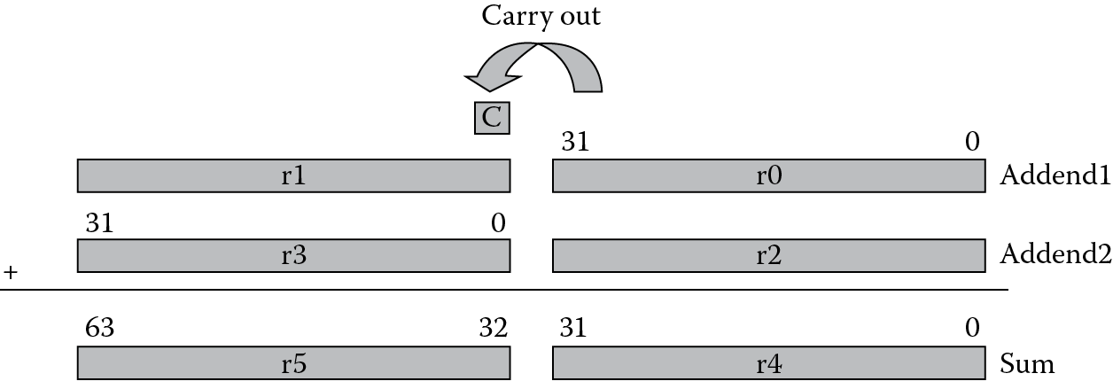
From the discussion on flags we noted that the Carry flag could be used to indicate that an operation produced a carry bit in the most significant bit of the result. The ADC, SUBC, and RSC instructions make use of this flag by adding the Carry flag into the operation. Suppose we wish to perform a 64-bit addition. Since the registers are only 32 bits wide, we would need to store the two addends in two registers each, and the sum would have to be stored in two registers.
Example 7.8
The following two instructions add a 64-bit integer contained in registers r2 and r3 to another 64-bit integer contained in registers r0 and r1, and place the result in registers r4 and r5:
ADDS r4,r0,r2 ; adding the least significant words
ADC r5,r1,r3 ; adding the most significant words
You can see in Figure 7.6 that the carry out from the lower 32-bit sum is added into the upper 32-bit sum to produce the final 64-bit result.
Example 7.9
The second operand can make use of the barrel shifter when performing adds and subtracts, a topic we’ll explore more shortly, such as
SUB r0, r0, r2, LSL #2 ; r0 = r0 − (r2 <<2)
ADD r1, r1, r3, LSR #3 ; r1 = r1 + (r3 >>3)
There are two very unusual, but useful, instructions listed above: RSB and RSC, which are reverse subtracts. The reverse subtract instruction comes about from having a barrel shifter on only one of the busses going from the register bank to the main ALU, as shown earlier in Figure 7.4. Consider the case where we want to perform the following operation:
SUB r0, r2, r3, LSL #2 ; r0 = r2 – r3*4
We could do this quite easily with this single instruction. However, suppose we want modify (shift) register r2 before the subtraction instead of register r3. Since subtraction is not a commutative operation, i.e.,
x − y ≠ y − x, y,x ≠ 0
register r2 must somehow be made to appear on the bus that contains the barrel shifter. This is done using the reverse subtract operation, where the instruction would be written as
RSB r0, r3, r2, LSL #2 ; r0 = r2*4 – r3
This same instruction can be used to great effect, since the second operand can also be a constant, so you could conceivably subtract a register value from a constant, instead of the other way around.
Example 7.10
Write an ARM7TDMI assembly program to perform the function of absolute value. Register r0 will contain the initial value, and r1 will contain the absolute value. The pseudo-instruction would look like
ABS r1, r0
Try to use only two instructions (not counting instructions to terminate the program or any directives).
Solution
Recall that the absolute value function always returns a positive value for the argument, so f(x) = |x| just changes the sign of the argument if the value is negative. We can do this with one more instruction and one instruction to change the sign:
AREA Prog7a, CODE, READONLY
ENTRY
MOVS r1, r0
RSBLT r1, r1, #0
done B done
END
The program first sets the status flags to see if anything needs to be done. If the argument is zero, the result is zero. If the argument is negative (LT indicates Less Than zero, but we’ll cover this in more detail in Chapter 8), the reverse subtract instruction subtracts r1 from zero, effectively changing its sign. Notice the conditional execution of the RSB instruction, since a positive value will fail the condition of being less than zero.
7.4.4 Saturated Math Operations
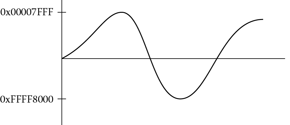
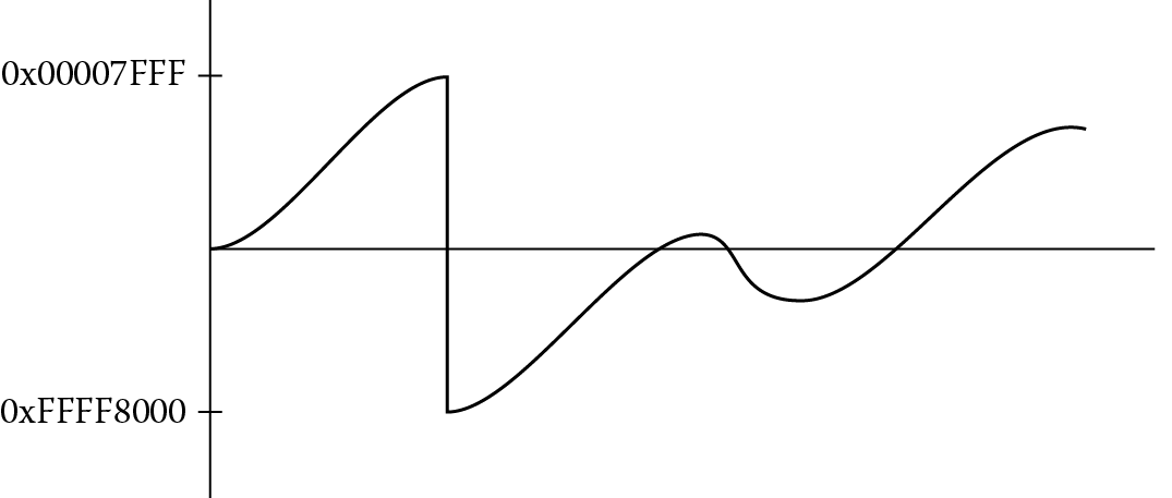
Algorithms for handling speech data, adaptive control algorithms, and routines for filtering are often sensitive to quantization effects when implemented on a microprocessor or microcontroller. A careful analysis of the both the implementation (e.g., direct or indirect, recursive or non-recursive) and the coefficients used in the filter gives programmers a better idea of precautions that must be made in advance. Sometimes it is required that limitations be placed on both the input data and the algorithm’s coefficients to prevent overflow conditions or to prevent an algorithm from becoming unstable. In other cases, the software can mitigate any problems by forcing intermediate values to stay within boundaries should they stray. Saturated math is one such approach, especially when dealing with signed data. For example, consider a digital waveform in Figure 7.7, possibly the output of an adaptive predictor, where the values are represented by 16-bit signed integers; in other words, the largest positive value in a register would be 0x00007FFF and the largest negative value would be 0xFFFF8000. If this signal were scaled in some way, it’s quite possible that the largest value would overflow, effectively flipping the MSB of a value so that a positive number suddenly becomes negative, and the waveform might appear as in Figure 7.8. Using saturated math instructions, the signal would get clipped, and the waveform might appear as in Figure 7.9, not correcting the values but at least keeping them within limits.
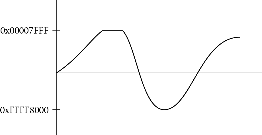
In version 6 cores and higher, many new instructions were added for manipulating saturated values, such as QADD, QADD8, QADD16, UQADD8, etc., and the Cortex-M4 includes addition, signed multiplication, subtraction, and parallel operations for working with saturated math, one of which we’ll examine in Section 7.5. These instructions will return maximum or minimum values based on the results of the operation if those values are exceeded. An additional status bit, the Q bit that we saw in Chapter 2, indicates that saturation has occurred and resides in the APSR shown in Figure 7.1. This bit is considered “sticky” in that once it is set, it must be written to a zero to clear it. In practice, you might use the saturated operation at the end of a loop or once data has been read as an input to an algorithm to ensure that values used in further processing are within acceptable limits.
Example 7.11
A 32-bit signed value is to be saturated into a 16-bit signed value. If the value in register r3 is 0x00030000, then the instruction
SSAT r4, #16, r3
will place the value 0x00007FFF into register r4, since the input value is above the threshold of 0x7FFF, and the Q bit will be set indicating that the value saturated. If the value in register r3 is 0xFFFF7FFF, then the returned value in register r4 would be 0xFFFF8000, since the initial value is below the threshold of 0xFFFF8000, the most negative number represented in 16 bits. Again, the Q bit is set.
Example 7.12
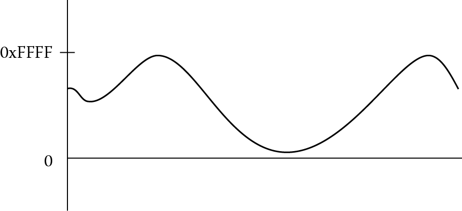
Unsigned saturation works analogously. Figure 7.10 shows a 16-bit signal where 0x0000 is the smallest value it would have and 0xFFFF is the largest. If register r3 contains the 32-bit signed value 0xFFFF8000, the unsigned saturation instruction
USAT r4, #16, r3
would return the value 0x00000000 and the Q bit is set, since the 32-bit signed input is well below the smallest unsigned value of zero. An input value of 0x00030000 would return 0x0000FFFF and the Q bit is set since the input exceeds the maximum unsigned value of 0xFFFF. See the ARM v7-M Architectural Reference Manual (ARM 2010a) for more detailed information about the use of SSAT and USAT.
7.4.5 Multiplication
Binary multiplication is provided on nearly every processor these days, but it comes at a cost. As an operation, it’s quite common. As a block of digital hardware, it’s expensive in that multipliers usually consume quite a bit of area and power relative to the other parts of a microprocessor. Older microcontrollers would often use a shift-add iterative routine to perform multiplication, avoiding building a large multiplier array; however, this tends to be quite slow. Modern designs usually perform multiplications in a single cycle or two, but again, because of power considerations, if there is a way to avoid using the array, an ARM compiler will try to produce code without multiply instructions, as we will see shortly. Microprocessors and/or DSP engines are often selected based on their ability to perform fast multiplication, especially in areas of speech and signal processing, signal analysis, and adaptive control.
Table 7.2 shows all of the supported instructions available in the ARM7TDMI, which are a small subset of those supported on the Cortex-M4. MUL and MLA are multiply and multiply-and-accumulate instructions that produce 32-bit results. MUL multiplies the values in two registers, truncates the result to 32 bits, and stores the product in a third register. MLA multiplies two registers, truncates the results to 32 bits, adds the value of a third register to the product, and stores the result in a fourth register, for example,
ARM7TDMI Multiply and Multiply-Accumulate Instructions
|
Instruction |
Comment |
|
MUL |
32x32 multiply with 32-bit product |
|
MLA |
32x32 multiply added to a 32-bit accumulated value |
|
SMULL |
Signed 32x32 multiply with 64-bit product |
|
UMULL |
Unsigned 32x32 multiply with 64-bit product |
|
SMLAL |
Signed 32x32 multiply added to a 64-bit accumulated value |
|
UMLAL |
Unsigned 32x32 multiply added to a 64-bit accumulated value |
MUL r4, r2, r1 ; r4 = r2 * r1
MULS r4, r2, r1 ; r4 = r2 * r1, then set the flags
MLA r7, r8, r9, r3 ; r7 = r8 * r9 + r3
Both MUL and MLA can optionally set the N and Z condition code flags. For multiplications that produce only 32 bits of result, there is no distinction between signed and unsigned multiplication. Only the least significant 32 bits of the result are stored in the destination register, and the sign of the operands does not affect this value. There is an additional multiply and subtract instruction (MLS) available on the Cortex-M4 which multiplies two 32-bit values together and then subtracts this product from a third value.
Example 7.13
Multiply long instructions produce 64-bit results. They multiply the values of two registers and store the 64-bit result in a third and fourth register. SMULL and UMULL are signed and unsigned multiply long instructions:
SMULL r4, r8, r2, r3 ; r4 = bits 31-0 of r2*r3
; r8 = bits 63-32 of r2*r3
UMULL r6, r8, r0, r1 ; {r8,r6} = r0*r1
These instructions multiply the values of two registers, add the 64-bit value from a third and fourth register, and store the 64-bit result in the third and fourth registers:
SMLAL r4, r8, r2, r3 ; {r8,r4} = r2*r3 + {r8,r4}
UMLAL r5, r8, r0, r1 ; {r8,r5} = r0*r1 + {r8,r5}
All four multiply long instructions can optionally set the N and Z condition code flags. If any source operand is negative, the most significant 32 bits of the result are affected.
7.4.6 Multiplication by a Constant
In our discussion of shifts and rotates, we saw that the inline barrel shifter in the ARM7TDMI’s datapath can be used in conjunction with other instructions, such as ADD or SUB, in effect getting a multiplication for free. This feature is used to its full advantage when certain multiplications are done using the barrel shifter instead of the multiplier array. Consider the case of multiplying a number by a power of two. This can be written using only an LSL instruction, i.e.,
LSL r1, r0, #2 ; r1 = r0*4
But what if we wanted to multiply two numbers, one of which is not a power of two, like five? Examine the following instruction:
ADD r0, r1, r1, LSL #2 ; r0 = r1 + r1*4
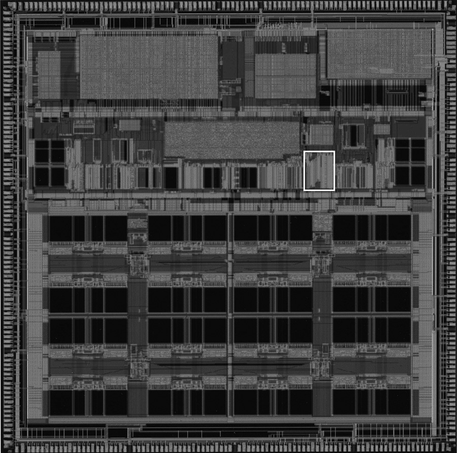
This is the same thing as taking a value, shifting it to the left two bits (giving a multiplication by four), and then adding the original value to the product. In other words, multiply the number by five. Why do it this way? Consider the size and power usage of a multiplier array, which is highlighted in Figure 7.11 for the ARM10200 microprocessor. In very low power applications, it’s often necessary to play every trick in the book to save power: not clocking logic that is not being used, powering down caches or the entire processor if it is not needed, reducing voltages and frequencies, etc. By using only the 32-bit adder and a barrel shifter, the ARM processors can actually generate multiplications by 2n, 2n − 1, and 2n + 1 in a single cycle, without having to use a multiplier array. This also potentially saves some execution time. For example,
RSB r0, r2, r2, LSL #3 ; r0 = r2*7
will perform a multiplication by 7 by taking register r2, shifting it left by 3 bits, yielding a multiplication by 8, and then subtracting register r2 from the product. Note that the reverse subtract instruction was used here, since an ordinary subtraction will produce the wrong result. By chaining together multiplications, for example, multiplying by 5 and then by 7, larger constants can be created. Examine the following code to see that you can, in fact, create multiplier arguments that are not powers of two:
ADD r0, r1, r1, LSL #1 ; r0 = r1*3
SUB r0, r0, r1, LSL #4 ; r0 = (r1*3) − (r1*16) = r1* − 13
ADD r0, r0, r1, LSL #7 ; r0 = (r1* − 13) + (r1*128) = r1*115
7.4.7 Division
Binary division is a subject that can get quite complicated very quickly. Historically, ARM cores did not include a binary integer divider in hardware, mostly because division is so infrequently used (and can therefore be done using a software routine), a divider can take up too much area and/or power to consider using on an embedded processor, and there are ways of avoiding division entirely. However, with denser geometries being made available to VLSI designers, it is possible to include division instructions in the newer ARM ISAs without too much overhead, and so we’ll examine the divider in the Cortex-M4. This is not to say that good software routines are not still available for processors like the ARM7TDMI. Factors to be considered in choosing a divider routine include the type of data you have (either fractional data or integer data), the speed of the algorithm needed, and the size of the code permitted to perform an algorithm in software. For an excellent treatment of the topic, consider reading Sloss, Symes, and Wright (2004). Runtime libraries include a division routine, so if you happen to be writing in C or C++, generally the compiler will take care of the division algorithm for you. But our focus is assembly, so we’ll consider at least one simple case.
The following code, which is a variation of a shift-subtract algorithm, can be used to divide two unsigned, 32-bit values, where the dividend is in register Ra and the divisor is in register Rb, producing a quotient in register Rc and a remainder in register Ra.
AREA Prog7b, CODE, READONLY
Rcnt RN 0 ; assign R0 to Rcnt
Ra RN 1 ; assign R1 to Ra
Rb RN 2 ; assign R2 to Rb
Rc RN 3 ; assign R3 to Rc
ENTRY
; Place your dividend in Ra
; Place your divisor in Rb
MOV Rcnt, #1 ; bit to control the
; division
Div1 CMP Rb, #0x80000000 ; move Rb until
; greater than Ra
CMPCC Rb, Ra
LSLCC Rb, Rb, #1
LSLCC Rcnt, Rcnt, #1
BCC Div1
MOV Rc, #0
Div2 CMP Ra, Rb ; test for possible
; subtraction
SUBCS Ra, Ra, Rb ; subtract if OK
ADDCS Rc, Rc, Rcnt ; put relevant bit
; into result
LSRS Rcnt, Rcnt, #1 ; shift control bit
LSRNE Rb, Rb, #1 ; halve unless
; finished
BNE Div2 ; divide result in Rc
; remainder in Ra
done B done
END
Example 7.14
Let’s compare the execution times using both the software routine above and the hardware divider on the Cortex-M4. We will divide 0xFF000000 by 0x98. Since these values can be created using two MOV instructions, load the registers Ra and Rb using:
MOV Ra, #0xFF000000 ; loads register r1
MOV Rb, #0x98 ; loads register r2
Running the code, register r3 contains the value 0x1AD7943 (the quotient) and register r1 contains 0x38 (the remainder). Using the Keil simulation tools, this code takes 450 cycles or 28.125 microseconds to complete on a Tiva TM4C123GH6ZRB microcontroller. Using three lines of code, we can reduce the execution time considerably:
MOV r1, #0xFF000000
MOV r2, #0x98
UDIV r3, r1, r2 ; r3 = r1/r2
Again, register r3 holds the quotient, but this code takes 0.813 microseconds, or 13 cycles!
The Cortex-M4 gives you the option to handle division by zero one of two ways: a fault exception or placing zero in the destination register. We’ll see an example in Chapter 15 showing how to configure the Nested Vectored Interrupt Controller (NVIC) to allow this type of exception.
7.5 DSP Extensions
The Cortex-M4 is the first M-class ARM core targeted at signal processing applications, and as such, offers more of the DSP instructions defined in the ARM v7-M Architectural Reference Manual (ARM 2010a) to handle cryptography routines, graphics algorithms, speech and video processing, etc. An instruction set summary can be found in the Cortex-M4 Technical Reference Manual (ARM 2009), detailing the behavior of each instruction. In this section, we’ll look at two examples of DSP operations that go beyond the usual multiply-accumulate calculations found in digital filters.
Example 7.15
Some instructions are designed for particular algorithms; some instructions are designed to work on certain types of data, for example on Q31 formatted data (to be explained shortly). Figure 7.12 shows how the instructions SMMLA and SMMLAR work. They both take two 32-bit operands and multiply them together. The most-significant word of the product is then added to a 32-bit accumulated value. If the R bit in the instruction is set (SMMLAR does this), then the value 0x80000000 is added prior to the truncation of the final result. Otherwise, nothing is added before truncation. For example, if we loaded registers r2 and r3 with 32-bit signed operands, and we used register r4 as an accumulated value, then
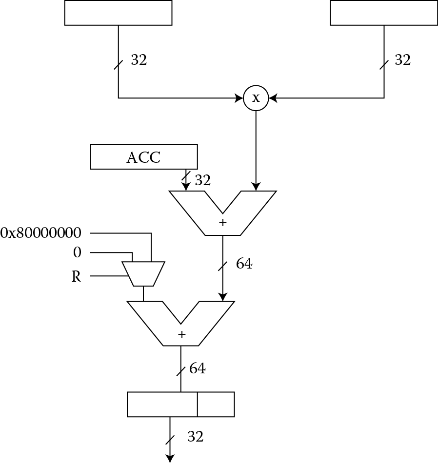
LDR r3, =0xFFFE6487
LDR r2, =0x80008F71;
LDR r4, =0xFFFF0003; accumulator
SMMLAR r9, r2, r3, r4
will produce the final result of 0xFFFFCDBF in register r9 as follows. The 32-bit multiply would produce the 64-bit product 0x0000CDBB9971C897. The accumulator value 0xFFFF0003 is then added producing the intermediate result:
Because we have selected the rounding version of the instruction, 0x80000000 is added to the sum, giving us
At this point, the upper 32 bits are kept, so that register r9 contains 0xFFFFCDBF.
Example 7.16
Without context, the USAD8 and USADA8 instructions make little sense, as they’re quite specific. These operations calculate the sum of absolute differences and the accumulated sum of absolute differences, respectively. It turns out that these calculations are useful for object recognition, motion estimation, and graphic compression algorithms, such as MPEG and H.264. When comparing two images, one simple block metric that can be found is the L1 norm of the difference image (or the Manhattan distance between two images), so if you wanted to compare, for example, image blocks of N × N squares in one image, say m1, with another N × N square in image m2 at a particular point (x,y), then you might compute the accumulated sum of absolute differences according to:
Four 8-bit pixel values can be read from each of two registers, say registers r3 and r4. The absolute differences are then found between corresponding bytes in registers r3 and r4. These four values are then summed in a destination register with the instruction
USAD8{<cond>} Rd, Rm, Rs ; sum of absolute differences
If you were to calculate an accumulated value, you could then follow at some point in your code with
USADA8{<cond>} {Rd,} Rm, Rs, Rn ; Rn is accumulated value to include
For both of these instructions, {<cond>} refers to an optional condition code that might be used (see Chapter 8).
7.6 Bit Manipulation Instructions
There are instructions in the Cortex-M4 that allow the manipulation of individual bits in a register: BFI (Bit Field Insert), UBFX (Unsigned Bit Field Extract), SBFX (Signed Bit Field Extract), BFC (Bit Field Clear), and RBIT (Reverse Bit order). Industrial and automotive applications typically require processing large amounts of general-purpose I/O data, and cycles can be wasted just moving individual bits around from sensors or other interfaces. In older architectures, it was necessary to use several instructions to copy contents, modify bits, and then store them; now with a single instruction, fields can be modified or extracted without changing the entire bit pattern in a register.
BFI, SBFX, and UBFX have the following syntax:
BFI{<cond>} <Rd>, <Rn>, <#lsb>, <#width>
SBFX{<cond>} <Rd>, <Rn>, <#lsb>, <#width>
UBFX{<cond>} <Rd>, <Rn>, <#lsb>, <#width>
BFC has the following syntax:
BFC{<cond>} <Rd>, <#lsb>, <#width>
RBIT is the simplest, and has the syntax:
RBIT{<cond>} <Rd>, <Rn>
The parameter #lsb indicates the least significant bit of the bitfield (in other words, where to start in the bit pattern going from right to left) and should be in the range of 0 to 31. The #width parameter indicates the width of the bitfield; this parameter should be in the range of 1 to (32-lsb). This makes the most significant bit position of the field lsb + width-1.
Suppose we start with register r0 equal to 0xABCDDCBA and register r1 equal to 0xFFFFFFFF. If we employ the instruction
BFI r1, r0, #8, #8
then registers r0 and r1 would appear as
|
r0 before |
r0 after |
|
0xABCDDCBA |
0xABCDDCBA |
|
r1 before |
r1 after |
|
0xFFFFFFFF |
0xFFFFBAFF |
The 8 lower bits of register r0 are inserted into register r1, starting at bit 8. Signed and unsigned bit field extract instructions work in a similar fashion. The instruction
UBFX r1, r0, #12, #8
takes an unsigned bit field from a register (inserting zeros), and it leaves register r0 and r1 as follows:
|
r0 before |
r0 after |
|
0xABCDDCBA |
0xABCDDCBA |
|
r1 before |
r1 after |
|
0xFFFFBAFF |
0x000000DD |
Figure 7.13 shows the operation. Signed bit field extract sign extends the most significant bit of the field before inserting it into a register. Clearing a bit field can be done using BFC, so if we wished to clear out a nibble from register r1, we would say
BFC r1, #4, #4
which leaves register r1 as
|
r1 before |
r1 after |
|
0x000000DD |
0x0000000D |
Should it become necessary to reverse the bit order of an entire register, you can use RBIT. The instruction
RBIT r1, r1
would produce the following results:
|
r1 before |
r1 after |
|
0x0000000D |
0xB0000000 |
7.7 Fractional Notation
When learning assembly, one of the first issues that often arises is how to put values like e and π in a program. This is a question of importance, given that you are likely to come across a value such as in practical code, and clearly the ARM processor works only with 32-bit integer values unless you have a floating-point unit available. Or does it? As we’ve seen in Chapter 1, the processor works with data, raw numbers, bit patterns. These bit patterns are interpreted as different things by the programmer, not the processor (unless specifically told to do so). Suppose you have the 32-bit value 0xF320ABCD in register r3. Is this number positive or negative? Under normal circumstances, you simply don’t know. You could interpret this number as −215,962,675 in decimal if it were a two’s complement representation. You could also interpret this as 4,079,004,621 if it were just an ordinary, unsigned integer. These decisions are largely based on the algorithm and the type of arithmetic operations that are being done on these numbers. Normally, the program expects data in a particular form and uses it accordingly—if an adaptive filter routine is written using only signed numbers, then the programmer takes care to treat the results as signed values.
To take this argument one step further, where is the binary point in the number 0xF320ABCD? In other words, where does the integer portion of this number start and where does the fractional portion start? Does it even have a fractional portion? Again, the answer lies with the programmer. It is useful at this point to look at small values first and then generalize the ideas to 32-bit numbers.
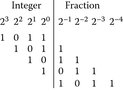
If the binary number 1011 is considered to be an unsigned number, the base 10 equivalent is 8 + 2 + 1 = 11. However, you could also assume that a binary point exists just before the last digit, as shown in Figure 7.14, which means that 101.1 would equal 4 + 1 + 0.5 = 5.5. This representation only gives two possible values for a fractional part—0 or 0.5, which isn’t terribly useful. If the binary point is assumed to be one more place to the left, the number becomes 10.11, which is 2 + 0.5 + 0.25 = 2.75 in base 10. Notice now that the two bits to the right of the binary point provide the four possibilities for a fractional value: 0, 0.25, 0.5, or 0.75. The resolution of the fraction is now 0.25, or in other words, the difference between any two fractional values can be no less than 0.25. Moving the binary point all the way to the left gives us the number 0.1011, which is 0.5 + 0.125 + 0.0625 = 0.6875 in base ten. Having an entirely fractional value is limiting in some ways, but the resolution of our fractional value is 0.0625, which is something of an improvement.
Recall from Chapter 1 that if a base ten number n is represented as an m-bit two’s complement number, with b being an individual bit’s value, the value is calculated as
so an 8-bit, two’s complement number such as 101100102 equals
−27 + 25 + 24 + 21 = −78.
But we just said that the binary point in any representation is entirely up to the programmer. So what if we assumed that this 8-bit number was divided by 27? The bit pattern is identical—the interpretation is different. It turns out that the base 10 number n would be calculated as
n = −1 + 2−2 + 2−3 + 2−6 = −0.609375.
In fact, we could divide any m-bit number by 2m−1, giving us just a fractional value n, such that
−1 ≤ n ≤ (1 − 2−(m−1)).
Going back to our question about e and π, if we wanted to represent a number with only some fractional part, then we could scale the number by something less than 2m−1. Suppose we have 16 bits, and we want to use e in a calculation. We know there are at least two bits needed to represent the integer portion of it (since the number is 2.71828…), so we would have at most 13 bits left for the fraction, given that the most-significant bit is the sign bit. In the literature, sometimes this is called Q notation, where our number might be called a Q13 number. Fortunately, the rules for working with Q-notated numbers are straightforward. Numbers that are added or subtracted in this notation should always have their binary points aligned, so Qn + Qn = Qn. When two numbers are multiplied, a Qn number times a Qm number will produce a result in a Q(n + m) format.
Example 7.17
Convert the transcendental number e into a Q13 format.
Solution
To produce e in Q13 notation, take the value e, multiply it by 213, and then convert this number to hexadecimal (here, a calculator is often handy). So we have
e × 213 = 22,268.1647 = 0x56FC.
Note we convert only the integer portion to hex. If this number is interpreted in Q13 notation, we can see that we do indeed have two bits to the left of the imaginary binary point and 13 bits to the right:
Example 7.18
Convert into a Q15 format.
Solution
We want our value to have 15 bits of fraction and one sign bit, or something that looks like
s.f14f13f12f11f10f9f8f7f6f5f4f3f2f1f0
First, we compute the decimal value for which turns out to be 0.8660254038. Now multiply this value times 215, giving 28,377.9204. Convert only the integer portion to a hexadecimal value, giving 0x6ED9.
Example 7.19
Let’s take our illustration one step further to actually have the machine calculate e times We need to convert this second number into fractional notation, too, so let’s use Q13 notation again. If the same rules above are followed, the Q13 representation of is 0x2D41. This short block of code below will perform the multiplication.
LDR r3, =0x56FC ; e in Q13 notation
LDR r2, =0x2D41 ; sqrt(2) in Q13 notation
MUL r5, r2, r3 ; product is in Q26 notation
If you run the code, you should find the value 0xF6061FC in register r5. Since the product is now in Q26 notation, we must convert the value to decimal and then divide by 226 for the final result, which turns out to be 3.84412378. The actual product is 3.84423102, but you would expect that some precision would be lost immediately from the original values being represented in a limited-precision notation. If there were an infinite number of bits available to perform the operation, then our results would be exact. We haven’t said what you would do with this value sitting in the register—yet. That 32-bit number could still represent just a big positive number or something odd like a mask for a configuration register in a cache controller! The processor has no idea what you’re doing.
Example 7.20
Let’s do another example, except this time one of the operands is negative, as this introduces a few more twists in handling these notations. The two values to be multiplied are π/4 and the value of a digital signal, say −0.3872. The two values should be in Q15 notation, represented by 16 bits. In other words, the representation looks like
s.f14f13f12f11f10f9f8f7f6f5f4f3f2f1f0,
or one sign bit, one imaginary binary point, and 15 bits of fractional value. To convert π/4 into a Q15 representation, we do as before, taking the decimal value and multiplying by 215, giving
π/4 × 215 = 25,735.927 = 0x6487 (convert only the integer portion to hex)
The other, negative number will require a little more thinking. The easiest way to handle negative numbers is to convert a positive value first, then negate the result. So, to convert a positive Q15 value first, we have
|−0.3872| × 215 = 12,687.7696 = 0x318F.
To negate 0x318F, you can either do it by hand (not recommended) or use a calculator or computer to perform a two’s complement negation. What results is a 16-bit value with the most significant bit set—it had better be, or the value isn’t negative. So negating 0x318F produces 0xCE71. (As an aside, some calculators will sign extend this value—just remember that you’ve chosen only 16 bits to represent the number!) As a sanity check, we can look at this value as
|
s |
f |
f |
f |
f |
f |
f |
f |
f |
f |
f |
f |
f |
f |
f |
f |
|
|
1 |
• |
1 |
0 |
0 |
1 |
1 |
1 |
0 |
0 |
1 |
1 |
1 |
0 |
0 |
0 |
1 |
|
↑ |
2−1 |
2−2 |
2−3 |
2−4 |
2−5 |
2−6 |
2−7 |
2−8 |
2−9 |
2−10 |
2−11 |
2−12 |
2−13 |
2−14 |
2−15 |
|
|
imaginary binary point |
||||||||||||||||
Since we said earlier that this could be viewed as
− 1 + 2−1 + 2−4 + 2−5 + 2−6 + … =
− 1 + 0.6128 = −0.3871765,
we’re getting what we expect. To code the multiplication, we do the same thing as before, only you must sign extend the negative operands to 32 bits if you use the ARM7TDMI. Why? The multiplier in the ARM7TDMI will take two 32-bit operands and multiply them together (returning only the lower 32 bits if the MUL instruction is used), so if we put a 16-bit value in one of the registers, the results will not be correct, as this is effectively a positive, two’s complement number in 32 bits—to the processor anyway. The first simulation uses the version 4T instruction set, so it’s necessary to do things the slightly old-fashioned way. The code would look like the following:
LDR r3, =0x6487 ; pi/4 in Q15 notation
LDR r2, =0xFFFFCE71 ; −0.3872 in Q15 notation
MUL r5, r2, r3 ; product is in Q30 notation
LSL r5, r5, #1 ; shift out extra sign bit
The result you find in register r5 is 0xD914032E. To interpret this number, it’s easiest to negate it first (again, use a calculator), giving 0x26EBFCD2, since we know the result is a negative number. It’s also a Q31 representation, so convert to base ten and then divide by 231, giving 0.3041. Why the extra shift at the end? Remember that a multiplication by two Q15 numbers will result in a Q30 product; however, there are 32 bits of result, which means that we end up with a superfluous sign bit in the most significant bit. In order to align the binary point again, everything is shifted left one bit. The final result could be taken from the upper half-word (16 bits) of register r5, resulting in another Q15 number. We didn’t see this shifting in the first example because the operands were positive (hence there was no sign bit set) and we didn’t do any realigning—we just stopped with a positive Q26 number.
If you use the Cortex-M4 processor, which has newer instructions that take 16-bit values and sign extend them for you, then you don’t need to add the extra bits to the operands. You would use the instruction SMULBB, which tells the processor that you want to take the bottom half of two registers, multiply them together, and treat all the values as signed two’s complement values. The code would be:
LDR r3, =0x6487 ; pi/4 in Q15 notation
LDR r2, =0xCE71 ; −0.3872 in Q15 notation
SMULBB r5, r2, r3 ; product is in Q30 notation
LSL r5, r5, #1 ; shift one bit left
done B done
Depending on the application and the precision needed in an algorithm, the data may be truncated at some point. So for graphics data where all the values may range only from 0 to 0xFF, once the algorithm produces a result, the entire fractional portion may be truncated anyway before the result is stored. For audio data or variables in a digital controller, you might keep some or all of the fractional precision before sending the result to a digital-to-analog converter (DAC), for example. The application will have a great influence on the way you handle the data. For further reading, see (Hohl and Hinds 2008; Oshana 2006).
7.8 Exercises
- What’s wrong with the following ARM instructions? You may want to consult the ARM Architectural Reference Manual to see the complete instruction descriptions and limitations.
- ADD r3, r7, #1023
- SUB r11, r12, r3, LSL #32
- RSCLES r0, r15, r0, LSL r4
- EORS r0, r15, r3, ROR r6
- Without using the MUL instruction, give instructions that multiply register r4 by:
- 135
- 255
- 18
- 16,384
- Write a compare routine to compare two 64-bit values, using only two instructions. (Hint: the second instruction is conditionally executed, based on the first comparison.)
- Write shift routines that allow you to arithmetically shift 64-bit values that are stored in two registers. The routines should shift an operand left or right by one bit.
- Write the following decimal values in Q15 notation:
- 0.3487
- −0.1234
- −0.1111
- 0.7574
- Write the following signed, two’s complement Q8 values in decimal:
- 0xFE32
- 0x9834
- 0xE800
- 0xF000
- Write the assembly code necessary to detect an error in a 12-bit Hamming code, where your code tests the 4 checksum bits c3, c2, c1, and c0. Place your corrupted data in memory. Assume that only a single error occurs in the data and store your corrected value in register r6.
- Write a program to calculate π × 48.9 in Q10 notation.
- Show the representation of sin(82°) in Q15 notation.
- Show the representation of sin(193°) in Q15 notation.
- Temperature conversion between Celsius and Fahrenheit can be computed using the relationship
- where C and F are in degrees. Write a program that converts a Celsius value in register r0 to degrees Fahrenheit. Convert the fraction into a Q15 representation and use multiplication instead of division in your routine. Load your test value from a memory location called CELS and store the result in memory labeled FAHR. Remember that you will need to specify the starting address of RAM for the microcontroller that you use in simulation. For example, the LPC2132 microcontroller has SRAM starting at address 0x40000000.
- Write a program for either the ARM7TDMI or the Cortex-M4 that counts the number of ones in a 32-bit value. Store the result in register r3.
- Using the ARM Architectural Reference Manual (or the Keil or CCS tools), give the bit pattern for the following ARM instructions:
- RSB r0, r3, r2, LSL #2
- SMLAL r3, r8, r2, r4
- ADD r0, r0, r1, LSL #7
- A common task that microcontrollers perform is ASCII-to-binary conversion. If you press a number on a keypad, for example, the processor receives the ASCII representation of that number, not the binary representation. A small routine is necessary to convert the data into binary for use in other arithmetic operations. Looking at the ASCII table in Appendix C, you will notice that the digits 0 through 9 are represented with the ASCII codes 0x30 to 0x39. The digits A through F are coded as 0x41 through 0x46. Since there is a break in the ranges, it’s necessary to do the conversion using two checks.
- The algorithm to do the conversion is
Mask away the parity bit (bit 7 of the ASCII representation), since we don’t care about it.
Subtract a bias away from the ASCII value.
Test to see if the digit is between 0 and 9.
If so, we’re done. Otherwise subtract 7 to find the value.
- Write this routine in assembly. You may assume that the ASCII representation is a valid character between 0 and F.
- Write four different instructions that clear register r7 to zero.
- Suppose register r0 contains the value 0xBBFF0000. Give the Thumb-2 instruction and register value for r1 that would insert the value 0x7777 into the lower half of register r0, so that the final value is 0xBBFF7777.
- Write ARM instructions that set bits 0, 4, and 12 in register r6 and leave the remaining bits unchanged.
- Write a program that converts a binary value between 0 and 15 into its ASCII representation. See Exercise 14 for background information.
- Assume that a signed long multiplication instruction is not available on the ARM7TDMI. Write a program that performs a 32 × 32 multiplication, producing a 64-bit result, using only UMULL and logical operations. Run the program to verify its operation.
- Write a program to add 128-bit numbers together, placing the result in registers r0, r1, r2, and r3. The first operand should be placed in registers r4, r5, r6, and r7, and the second operand should be in registers r8, r9, r10, and r11.
- Write a program that takes character data “a” through “z” and returns the character in uppercase.
- Give three different methods to test the equivalence of two values held in registers r0 and r1.
- Write assembly code for the ARM7TDMI to perform the following signed division:
r1 = r0/16
- Multiply 0xFFFFFFFF (−1 in a two’s complement representation) and 0x80000000 (the largest negative number in a 32-bit two’s complement representation) on the ARM7TDMI. Use the MUL instruction. What value do you get? Does this number make sense? Why or why not?
- A Gray code is an ordering of 2n binary numbers such that only one bit changes from one entry to the next. One example of a 2-bit Gray code is 10 11 01 002. The spaces in this example are for readability. Write ARM assembly to turn a 2-bit Gray code held in register r1 into a 3-bit Gray code in register r2. Note that the 2-bit Gray code occupies only bits [7:0] of register r1, and the 3-bit Gray code occupies only bits [23:0] of register r2. You can ignore the leading zeros. One way to build an n-bit Gray code from an (n − 1)-bit Gray code is to prefix every (n − 1)-bit element of the code with 0. Then create the additional n-bit Gray code elements by taking each (n − 1)-bit Gray code element in reverse order and prefixing it with a one. For example, the 2-bit Gray code above becomes
010 011 001 000 100 101 111 110
- Write a program that calculates the area of a circle. Register r0 will contain the radius of the circle in Q3 notation. Represent π in Q10 notation, and store the result in register r3 in Q3 notation.
* Since older ARM7TDMI code is quite common, it is very likely you will see both formats of instruction.