Table of Contents for
ARM Assembly Language, 2nd Edition
 ARM Assembly Language, 2nd Edition
Published by
Chapman and Hall/CRC, 2016
ARM Assembly Language, 2nd Edition
Published by
Chapman and Hall/CRC, 2016
- Contents
- ARM Assembly Language: Fundamentals and Techniques, Second Edition
- Preliminaries
- To our families
- Preface
- Acknowledgments
- Authors
- Chapter 1 - An Overview of Computing Systems
- Chapter 2 - The Programmer’s Model
- Chapter 3 - Introduction to Instruction Sets: v4T and v7-M
- Chapter 4 - Assembler Rules and Directives
- Chapter 5 - Loads, Stores, and Addressing
- Chapter 6 - Constants and Literal Pools
- Chapter 7 - Integer Logic and Arithmetic
- Chapter 8 - Branches and Loops
- Chapter 9 - Introduction to Floating-Point: Basics, Data Types, and Data Transfer
- Chapter 10 - Introduction to Floating-Point: Rounding and Exceptions
- Chapter 11 - Floating-Point Data-Processing Instructions
- Chapter 12 - Tables
- Chapter 13 - Subroutines and Stacks
- Chapter 14 - Exception Handling: ARM7TDMI
- Chapter 15 - Exception Handling: v7-M
- Chapter 16 - Memory-Mapped Peripherals
- Chapter 17 - ARM, Thumb and Thumb-2 Instructions
- Chapter 18 - Mixing C and Assembly
- Appendix A: Running Code Composer Studio
- Appendix B: Running Keil Tools
- Appendix C: ASCII Character Codes
- Appendix D
- Glossary
- References
Chapter 1
An Overview of Computing Systems
1.1 Introduction
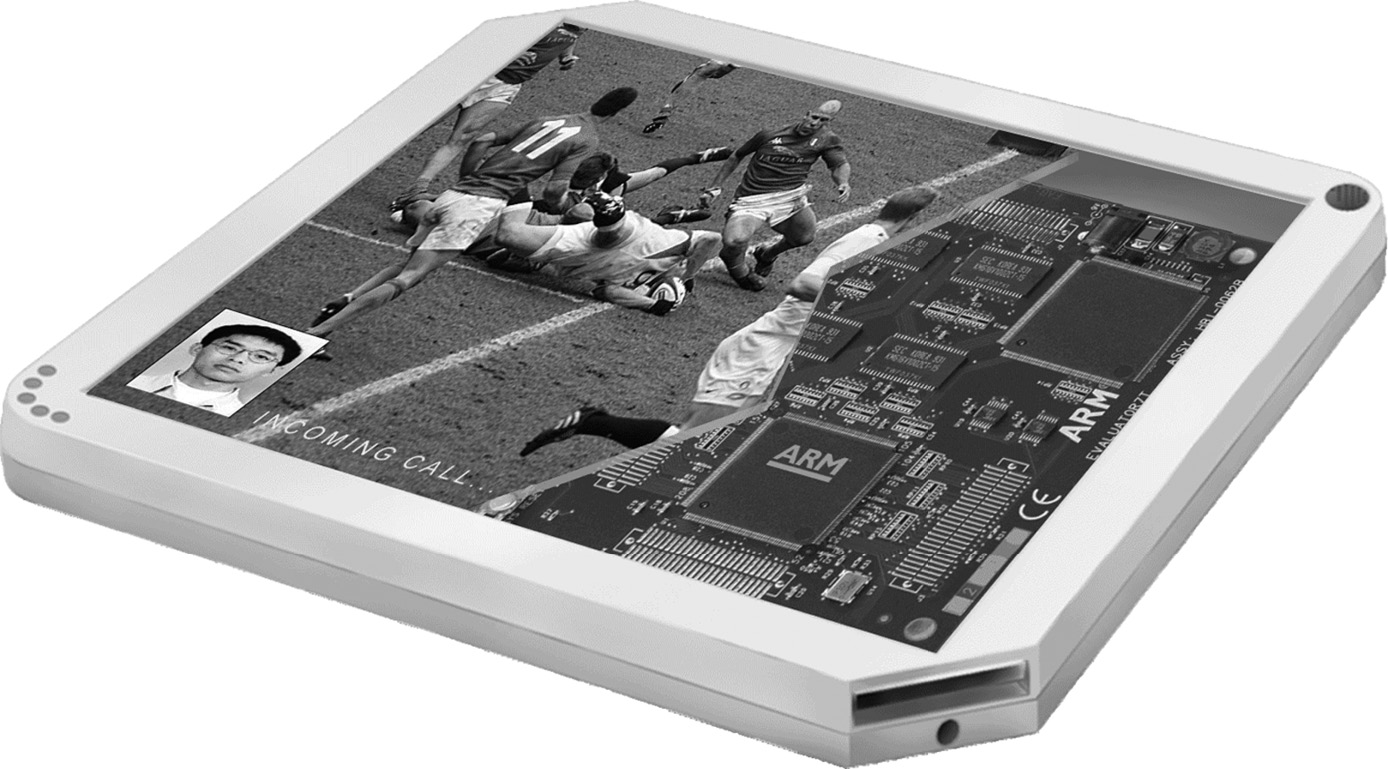
Most users of cellular telephones don’t stop to consider the enormous amount of effort that has gone into designing an otherwise mundane object. Lurking beneath the display, below the user’s background picture of his little boy holding a balloon, lies a board containing circuits and wires, algorithms that took decades to refine and implement, and software to make it all work seamlessly together. What exactly is happening in those circuits? How do such things actually work? Consider a modern tablet, considered a fictitious device only years ago, that displays live television, plays videos, provides satellite navigation, makes international Skype calls, acts as a personal computer, and contains just about every interface known to man (e.g., USB, Wi-Fi, Bluetooth, and Ethernet), as shown in Figure 1.1. Gigabytes of data arrive to be viewed, processed, or saved, and given the size of these hand-held devices, the burden of efficiency falls to the designers of the components that lie within them.
Underneath the screen lies a printed circuit board (PCB) with a number of individual components on it and probably at least two system-on-chips (SoCs). A SoC is nothing more than a combination of processors, memory, and graphics chips that have been fabricated in the same package to save space and power. If you further examine one of the SoCs, you will find that within it are two or three specialized microprocessors talking to graphics engines, floating-point units, energy management units, and a host of other devices used to move information from one device to another. The Texas Instruments (TI) TMS320DM355 is a good example of a modern SoC, shown in Figure 1.2.
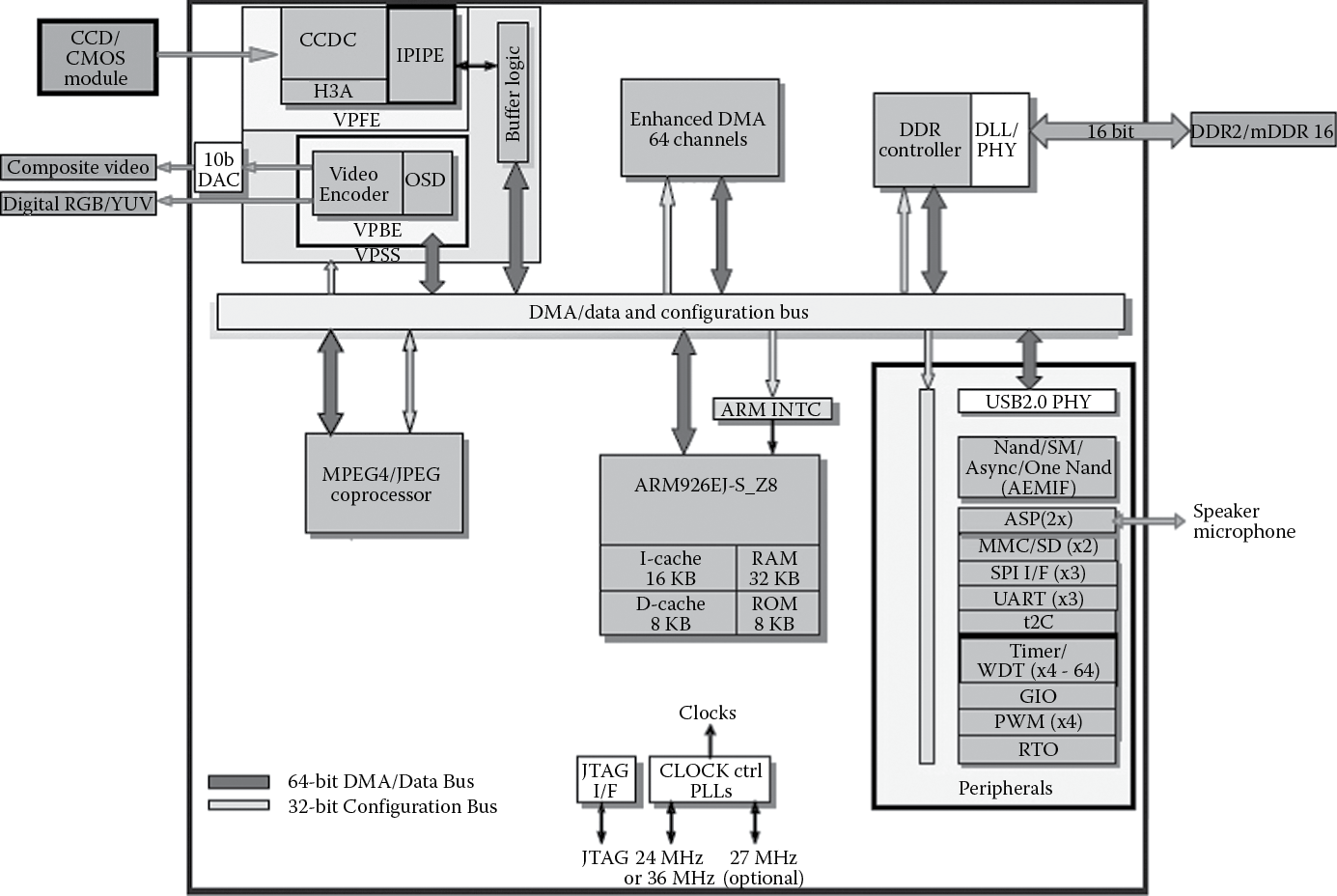
The TMS320DM355 System-on-Chip from Texas Instruments. (From Texas Instruments. With permission.)
System-on-chip designs are becoming increasingly sophisticated, where engineers are looking to save both money and time in their designs. Imagine having to produce the next generation of our hand-held device—would it be better to reuse some of our design, which took nine months to build, or throw it out and spend another three years building yet another, different SoC? Because the time allotted to designers for new products shortens by the increasing demand, the trend in industry is to take existing designs, especially designs that have been tested and used heavily, and build new products from them. These tested designs are examples of “intellectual property”—designs and concepts that can be licensed to other companies for use in large projects. Rather than design a microprocessor from scratch, companies will take a known design, something like a Cortex-A57 from ARM, and build a complex system around it. Moreover, pieces of the project are often designed to comply with certain standards so that when one component is changed, say our newest device needs a faster microprocessor, engineers can reuse all the surrounding devices (e.g., MPEG decoders or graphics processors) that they spent years designing. Only the microprocessor is swapped out.
This idea of building a complete system around a microprocessor has even spilled into the microcontroller industry. A microprocessor can be seen as a computing engine with no peripherals. Very simple processors can be combined with useful extras such as timers, universal asynchronous receiver/transmitters (UARTs), or analog-to-digital (A/D) converters to produce a microcontroller, which tends to be a very low-cost device for use in industrial controllers, displays, automotive applications, toys, and hundreds of other places one normally doesn’t expect to find a computing engine. As these applications become more demanding, the microcontrollers in them become more sophisticated, and off-the-shelf parts today surpass those made even a decade ago by leaps and bounds. Even some of these designs are based on the notion of keeping the system the same and replacing only the microprocessor in the middle.
1.2 History of RISC
Even before computers became as ubiquitous as they are now, they occupied a place in students’ hearts and a place in engineering buildings, although it was usually under the stairs or in the basement. Before the advent of the personal computer, mainframes dominated the 1980s, with vendors like Amdahl, Honeywell, Digital Equipment Corporation (DEC), and IBM fighting it out for top billing in engineering circles. One need only stroll through the local museum these days for a glimpse at the size of these machines. Despite all the circuitry and fans, at the heart of these machines lay processor architectures that evolved from the need for faster operations and better support for more complicated operating systems. The DEC VAX series of minicomputers and superminis—not quite mainframes, but larger than minicomputers—were quite popular, but like their contemporary architectures, the IBM System/38, Motorola 68000, and the Intel iAPX-432, they had processors that were growing more complicated and more difficult to design efficiently. Teams of engineers would spend years trying to increase the processor’s frequency (clock rate), add more complicated instructions, and increase the amount of data that it could use. Designers are doing the same thing today, except most modern systems also have to watch the amount of power consumed, especially in embedded designs that might run on a single battery. Back then, power wasn’t as much of an issue as it is now—you simply added larger fans and even water to compensate for the extra heat!
The history of Reduced Instruction Set Computers (RISC) actually goes back quite a few years in the annals of computing research. Arguably, some early work in the field was done in the late 1960s and early 1970s by IBM, Control Data Corporation and Data General. In 1981 and 1982, David Patterson and Carlo Séquin, both at the University of California, Berkeley, investigated the possibility of building a processor with fewer instructions (Patterson and Sequin 1982; Patterson and Ditzel 1980), as did John Hennessy at Stanford (Hennessy et al. 1981) around the same time. Their goal was to create a very simple architecture, one that broke with traditional design techniques used in Complex Instruction Set Computers (CISCs), e.g., using microcode (defined below) in the processor; using instructions that had different lengths; supporting complex, multi-cycle instructions, etc. These new architectures would produce a processor that had the following characteristics:
- All instructions executed in a single cycle. This was unusual in that many instructions in processors of that time took multiple cycles. The trade-off was that an instruction such as MUL (multiply) was available without having to build it from shift/add operations, making it easier for a programmer, but it was more complicated to design the hardware. Instructions in mainframe machines were built from primitive operations internally, but they were not necessarily faster than building the operation out of simpler instructions. For example, the VAX processor actually had an instruction called INDEX that would take longer than if you were to write the operation in software out of simpler commands!
- All instructions were the same size and had a fixed format. The Motorola 68000 was a perfect example of a CISC, where the instructions themselves were of varying length and capable of containing large constants along with the actual operation. Some instructions were 2 bytes, some were 4 bytes. Some were longer. This made it very difficult for a processor to decode the instructions that got passed through it and ultimately executed.
- Instructions were very simple to decode. The register numbers needed for an operation could be found in the same place within most instructions. Having a small number of instructions also meant that fewer bits were required to encode the operation.
- The processor contained no microcode. One of the factors that complicated processor design was the use of microcode, which was a type of “software” or commands within a processor that controlled the way data moved internally. A simple instruction like MUL (multiply) could consist of dozens of lines of microcode to make the processor fetch data from registers, move this data through adders and logic, and then finally move the product into the correct register or memory location. This type of design allowed fairly complicated instructions to be created—a VAX instruction called POLY, for example, would compute the value of an nth-degree polynomial for an argument x, given the location of the coefficients in memory and a degree n. While POLY performed the work of many instructions, it only appeared as one instruction in the program code.
- It would be easier to validate these simpler machines. With each new generation of processor, features were always added for performance, but that only complicated the design. CISC architectures became very difficult to debug and validate so that manufacturers could sell them with a high degree of confidence that they worked as specified.
- The processor would access data from external memory with explicit instructions—Load and Store. All other data operations, such as adds, subtracts, and logical operations, used only registers on the processor. This differed from CISC architectures where you were allowed to tell the processor to fetch data from memory, do something to it, and then write it back to memory using only a single instruction. This was convenient for the programmer, and especially useful to compilers, but arduous for the processor designer.
- For a typical application, the processor would execute more code. Program size was expected to increase because complicated operations in older architectures took more RISC instructions to complete the same task. In simulations using small programs, for example, the code size for the first Berkeley RISC architecture was around 30% larger than the code compiled for a VAX 11/780. The novel idea of a RISC architecture was that by making the operations simpler, you could increase the processor frequency to compensate for the growth in the instruction count. Although there were more instructions to execute, they could be completed more quickly.
Turn the clock ahead 33 years, and these same ideas live on in most all modern processor designs. But as with all commercial endeavors, there were good RISC machines that never survived. Some of the more ephemeral designs included DEC’s Alpha, which was regarded as cutting-edge in its time; the 29000 family from AMD; and Motorola’s 88000 family, which never did well in industry despite being a fairly powerful design. The acronym RISC has definitely evolved beyond its own moniker, where the original idea of a Reduced Instruction Set, or removing complicated instructions from a processor, has been buried underneath a mountain of new, albeit useful instructions. And all manufacturers of RISC microprocessors are guilty of doing this. More and more operations are added with each new generation of processor to support the demanding algorithms used in modern equipment. This is referred to as “feature creep” in the industry. So while most of the RISC characteristics found in early processors are still around, one only has to compare the original Berkeley RISC-1 instruction set (31 instructions) or the second ARM processor (46 operations) with a modern ARM processor (several hundred instructions) to see that the “R” in RISC is somewhat antiquated. With the introduction of Thumb-2, to be discussed throughout the book, even the idea of a fixed-length instruction set has gone out the window!
1.2.1 ARM Begins
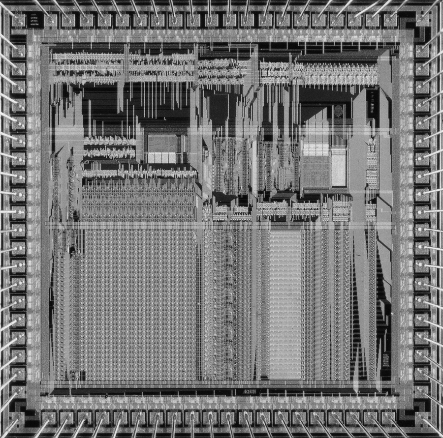
The history of ARM Holdings PLC starts with a now-defunct company called Acorn Computers, which produced desktop PCs for a number of years, primarily adopted by the educational markets in the UK. A plan for the successor to the popular BBC Micro, as it was known, included adding a second processor alongside its 6502 microprocessor via an interface called the “Tube”. While developing an entirely new machine, to be called the Acorn Business Computer, existing architectures such as the Motorola 68000 were considered, but rather than continue to use the 6502 microprocessor, it was decided that Acorn would design its own. Steve Furber, who holds the position of ICL Professor of Computer Engineering at the University of Manchester, and Sophie Wilson, who wrote the original instruction set, began working within the Acorn design team in October 1983, with VLSI Technology (bought later by Philips Semiconductor, now called NXP) as the silicon partner who produced the first samples. The ARM1 arrived back from the fab on April 26, 1985, using less than 25,000 transistors, which by today’s standards would be fewer than the number found in a good integer multiplier. It’s worth noting that the part worked the first time and executed code the day it arrived, which in that time frame was quite extraordinary. Unless you’ve lived through the evolution of computing, it’s also rather important to put another metric into context, lest it be overlooked—processor speed. While today’s desktop processors routinely run between 2 and 3.9 GHz in something like a 22 nanometer process, embedded processors typically run anywhere from 50 MHz to about 1 GHz, partly for power considerations. The original ARM1 was designed to run at 4 MHz (note that this is three orders of magnitude slower) in a 3 micron process! Subsequent revisions to the architecture produced the ARM2, as shown in Figure 1.3. While the processor still had no caches (on-chip, localized memory) or memory management unit (MMU), multiply and multiply-accumulate instructions were added to increase performance, along with a coprocessor interface for use with an external floating-point accelerator. More registers for handling interrupts were added to the architecture, and one of the effective address types was actually removed. This microprocessor achieved a typical clock speed of 12 MHz in a 2 micron process. Acorn used the device in the new Archimedes desktop PC, and VLSI Technology sold the device (called the VL86C010) as part of a processor chip set that also included a memory controller, a video controller, and an I/O controller.
1.2.2 The Creation of ARM Ltd.
In 1989, the dominant desktop architectures, the 68000 family from Motorola and the x86 family from Intel, were beginning to integrate memory management units, caches, and floating-point units on board the processor, and clock rates were going up—25 MHz in the case of the first 68040. (This is somewhat misleading, as this processor used quadrature clocks, meaning clocks that are derived from overlapping phases of two skewed clocks, so internally it was running at twice that frequency.) To compete in this space, the ARM3 was developed, complete with a 4K unified cache, also running at 25 MHz. By this point, Acorn was struggling with the dominance of the IBM PC in the market, but continued to find sales in education, specialist, and hobbyist markets. VLSI Technology, however, managed to find other companies willing to use the ARM processor in their designs, especially as an embedded processor, and just coincidentally, a company known mostly for its personal computers, Apple, was looking to enter the completely new field of personal digital assistants (PDAs).
Apple’s interest in a processor for its new device led to the creation of an entirely separate company to develop it, with Apple and Acorn Group each holding a stake, and Robin Saxby (now Sir Robin Saxby) being appointed as managing director. The new company, consisting of money from Apple, twelve Acorn engineers, and free tools from VLSI Technology, moved into a new building, changed the name of the architecture from Acorn RISC Machine to Advanced RISC Machine, and developed a completely new business model. Rather than selling the processors, Advanced RISC Machines Ltd. would sell the rights to manufacture its processors to other companies, and in 1990, VLSI Technology would become the first licensee. Work began in earnest to produce a design that could act as either a standalone processor or a macrocell for larger designs, where the licensees could then add their own logic to the processor core. After making architectural extensions, the numbering skipped a few beats and moved on to the ARM6 (this was more of a marketing decision than anything else). Like its competition, this processor now included 32-bit addressing and supported both big- and little-endian memory formats. The CPU used by Apple was called the ARM610, complete with the ARM6 core, a 4K cache, a write buffer, and an MMU. Ironically, the Apple PDA (known as the Newton) was slightly ahead of its time and did quite poorly in the market, partly because of its price and partly because of its size. It wouldn’t be until the late 1990s that Apple would design a device based on an ARM7 processor that would fundamentally change the way people viewed digital media—the iPod.
The ARM7 processor is where this book begins. Introduced in 1993, the design was used by Acorn for a new line of computers and by Psion for a new line of PDAs, but it still lacked some of the features that would prove to be huge selling points for its successor—the ARM7TDMI, shown in Figure 1.4. While it’s difficult to imagine building a system today without the ability to examine the processor’s registers, the memory system, your C++ source code, and the state of the processor all in a nice graphical interface, historically, debugging a part was often very difficult and involved adding large amounts of extra hardware to a system. The ARM7TDMI expanded the original ARM7 design to include new hardware specifically for an external debugger (the initials “D” and “I” stood for Debug and ICE, or In-Circuit Emulation, respectively), making it much easier and less expensive to build and test a complete system. To increase performance in embedded systems, a new, compressed instruction set was created. Thumb, as it was called, gave software designers the flexibility to either put more code into the same amount of memory or reduce the amount of memory needed for a given design. The burgeoning cell phone industry was quite keen to use this new feature, and consequently began to heavily adopt the ARM7TDMI for use in mobile handsets. The initial “M” reflected a larger hardware multiplier in the datapath of the design, making it suitable for all sorts of digital signal processing (DSP) algorithms. The combination of a small die area, very low power, and rich instruction set made the ARM7TDMI one of ARM’s best-selling processors, and despite its age, continues to be used heavily in modern embedded system designs. All of these features have been used and improved upon in subsequent designs.
Throughout the 1990s, ARM continued to make improvements to the architecture, producing the ARM8, ARM9, and ARM10 processor cores, along with derivatives of these cores, and while it’s tempting to elaborate on these designs, the discussion could easily fill another textbook. However, it is worth mentioning some highlights of this decade. Around the same time that the ARM9 was being developed, an agreement with Digital Equipment Corporation allowed it to produce its own version of the ARM architecture, called StrongARM, and a second version was slated to be produced alongside the design of the ARM10 (they would be the same processor). Ultimately, DEC sold its design group to Intel, who then decided to continue the architecture on its own under the brand XScale. Intel produced a second version of its design, but has since sold this design to Marvell. Finally, on a corporate note, in 1998 ARM Holdings PLC was floated on the London and New York Stock Exchanges as a publicly traded company.
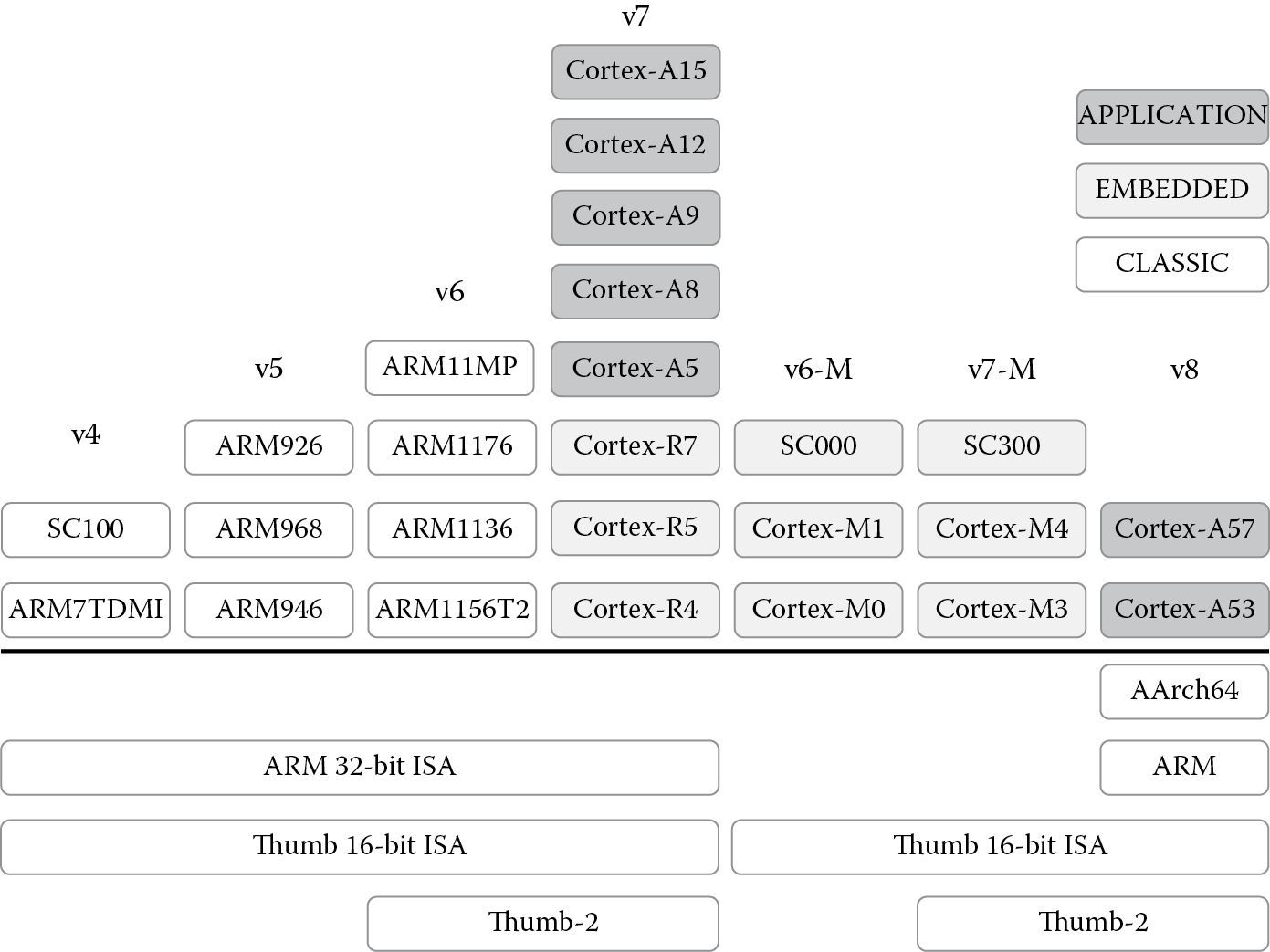
In the early part of the new century, ARM released several new processor lines, including the ARM11 family, the Cortex family, and processors for multi-core and secure applications. The important thing to note about all of these processors, from a programmer’s viewpoint anyway, is the version. From Figure 1.5, you can see that while there are many different ARM cores, the version precisely defines the instruction set that each core executes. Other salient features such as the memory architecture, Java support, and floating-point support come mostly from the individual cores. For example, the ARM1136JF-S is a synthesizable processor, one that supports both floating-point and Java in hardware; however, it supports the version 6 instruction set, so while the implementation is based on the ARM11, the instruction set architecture (ISA) dictates which instructions the compiler is allowed to use. The focus of this book is the ARM version 4T and version 7-M instruction sets, but subsequent sets can be learned as needed.
1.2.3 ARM Today
By 2002, there were about 1.3 billion ARM-based devices in myriad products, but mostly in cell phones. By this point, Nokia had emerged as a dominant player in the mobile handset market, and ARM was the processor powering these devices. While TI supplied a large portion of the cellular market’s silicon, there were other ARM partners doing the same, including Philips, Analog Devices, LSI Logic, PrairieComm, and Qualcomm, with the ARM7 as the primary processor in the offerings (except TI’s OMAP platform, which was based on the ARM9).
Application Specific Integrated Circuits (ASICs) require more than just a processor core—they require peripheral logic such as timers and USB interfaces, standard cell libraries, graphics engines, DSPs, and a bus structure to tie everything together. To move beyond just designing processor cores, ARM began acquiring other companies focusing on all of these specific areas. In 2003, ARM purchased Adelante Technologies for data engines (DSP processors, in effect). In 2004, ARM purchased Axys Design Automation for new hardware tools and Artisan Components for standard cell libraries and memory compilers. In 2005, ARM purchased Keil Software for microcontroller tools. In 2006, ARM purchased Falanx for 3D graphics accelerators and SOISIC for silicon-on-insulator technology. All in all, ARM grew quite rapidly over six years, but the ultimate goal was to make it easy for silicon partners to design an entire system-on-chip architecture using ARM technology.
Billions of ARM processors have been shipped in everything from digital cameras to smart power meters. In 2012 alone, around 8.7 billion ARM-based chips were created by ARM’s partners worldwide. Average consumers probably don’t realize how many devices in their pockets and their homes contain ARM-based SoCs, mostly because ARM, like the silicon vendor, does not receive much attention in the finished product. It’s unlikely that a Nokia cell phone user thinks much about the fact that TI provided the silicon and that ARM provided part of the design.
1.2.4 The Cortex Family
Due to the radically different requirements of embedded systems, ARM decided to split the processor cores into three distinct families, where the end application now determines both the nature and the design of the processors, but all of them go by the trade name of Cortex. The Cortex-A, Cortex-R, and Cortex-M families continue to add new processors each year, generally based on performance requirements as well as the type of end application the cores are likely to see. A very basic cell phone doesn’t have the same throughput requirements as a smartphone or a tablet, so a Cortex-A5 might work just fine, whereas an infotainment system in a car might need the ability to digitally sample and process very large blocks of data, forcing the SoC designer to build a system out of two or four Cortex-A15 processors. The controller in a washing machine wouldn’t require a 3 GHz processor that costs eight dollars, so a very lightweight Cortex-M0 solves the problem for around 70 cents. As we explore the older version 4T instructions, which operate seamlessly on even the most advanced Cortex-A and Cortex-R processors, the Cortex-M architecture resembles some of the older microcontrollers in use and requires a bit of explanation, which we’ll provide throughout the book.
1.2.4.1 The Cortex-A and Cortex-R Families
The Cortex-A line of cores focuses on high-end applications such as smart phones, tablets, servers, desktop processors, and other products which require significant computational horsepower. These cores generally have large caches, additional arithmetic blocks for graphics and floating-point operations, and memory management units to support large operating systems, such as Linux, Android, and Windows. At the high end of the computing spectrum, these processors are also likely to support systems containing multiple cores, such as those found in servers and wireless base stations, where you may need up to eight processors at once. The 32-bit Cortex-A family includes the Cortex-A5, A7, A8, A9, A12, and A15 cores. Newer, 64-bit architectures include the A57 and A53 processors. In many designs, equipment manufacturers build custom solutions and do not use off-the-shelf SoCs; however, there are quite a few commercial parts from the various silicon vendors, such as Freescale’s i.MX line based around the Cortex-A8 and A9; TI’s Davinci and Sitara lines based on the ARM9 and Cortex-A8; Atmel’s SAMA5D3 products based on the Cortex-A5; and the OMAP and Keystone multi-core solutions from TI based on the Cortex-A15. Most importantly, there are very inexpensive evaluation modules for which students and instructors can write and test code, such as the Beaglebone Black board, which uses the Cortex-A8.
The Cortex-R cores (R4, R5, and R7) are designed for those applications where real-time and/or safety constraints play a major role; for example, imagine an embedded processor designed within an anti-lock brake system for automotive use. When the driver presses on the brake pedal, the system is expected to have completely deterministic behavior—there should be no guessing as to how many cycles it might take for the processor to acknowledge the fact that the brake pedal has been pressed! In complex systems, a simple operation like loading multiple registers can introduce unpredictable delays if the caches are turned on and an interrupt comes in at the just the wrong time. Safety also plays a role when considering what might happen if a processor fails or becomes corrupted in some way, and the solution involves building redundant systems with more than one processor. X-ray machines, CT scanners, pacemakers, and other medical devices might have similar requirements. These cores are also likely to be asked to work with operating systems, large memory systems, and a wide variety of peripherals and interfaces, such as Bluetooth, USB, and Ethernet. Oddly enough, there are only a handful of commercial offerings right now, along with their evaluation platforms, such as TMS570 and RM4 lines from TI.
1.2.4.2 The Cortex-M Family
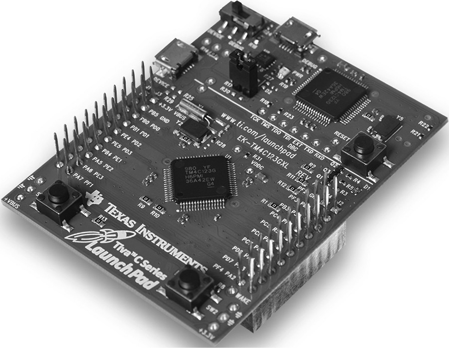
Finally, the Cortex-M line is targeted specifically at the world of microcontrollers, parts which are so deeply embedded in systems that they often go unnoticed. Within this family are the Cortex-M0, M0+, M1, M3, and M4 cores, which the silicon vendors then take and use to build their own brand of off-the-shelf controllers. As the much older, 8-bit microcontroller space moves into 32-bit processing, for controlling car seats, displays, power monitoring, remote sensors, and industrial robotics, industry requires a variety of microcontrollers that cost very little, use virtually no power, and can be programmed quickly. The Cortex-M family has surfaced as a very popular product with silicon vendors: in 2013, 170 licenses were held by 130 companies, with their parts costing anywhere from two dollars to twenty cents. The Cortex-M0 is the simplest, containing only a core, a nested vectored interrupt controller (NVIC), a bus interface, and basic debug logic. Its tiny size, ultra-low gate count, and small instruction set (only 56 instructions) make it well suited for applications that only require a basic controller. Commercial parts include the LPC1100 line from NXP, and the XMC1000 line from Infineon. The Cortex-M0+ is similar to the M0, with the addition of a memory protection unit (MPU), a relocatable vector table, a single-cycle I/O interface for faster control, and enhanced debug logic. The Cortex-M1 was designed specifically for FPGA implementations, and contains a core, instruction-side and data-side tightly coupled memory (TCM) interfaces, and some debug logic. For those controller applications that require fast interrupt response times, the ability to process signals quickly, and even the ability to boot a small operating system, the Cortex-M3 contains enough logic to handle such requirements. Like its smaller cousins, the M3 contains an NVIC, MPU, and debug logic, but it has a richer instruction set, an SRAM and peripheral interface, trace capability, a hardware divider, and a single-cycle multiplier array. The Cortex-M4 goes further, including additional instructions for signal processing algorithms; the Cortex-M4 with optional floating-point hardware stretches even further with additional support for single-precision floating-point arithmetic, which we’ll examine in Chapters 9, 10, and 11. Some commercial parts offering the Cortex-M4 include the SAM4SD32 controllers from Atmel, the Kinetis family from Freescale, and the Tiva C series from TI, shown in its evaluation module in Figure 1.6.
1.3 The Computing Device
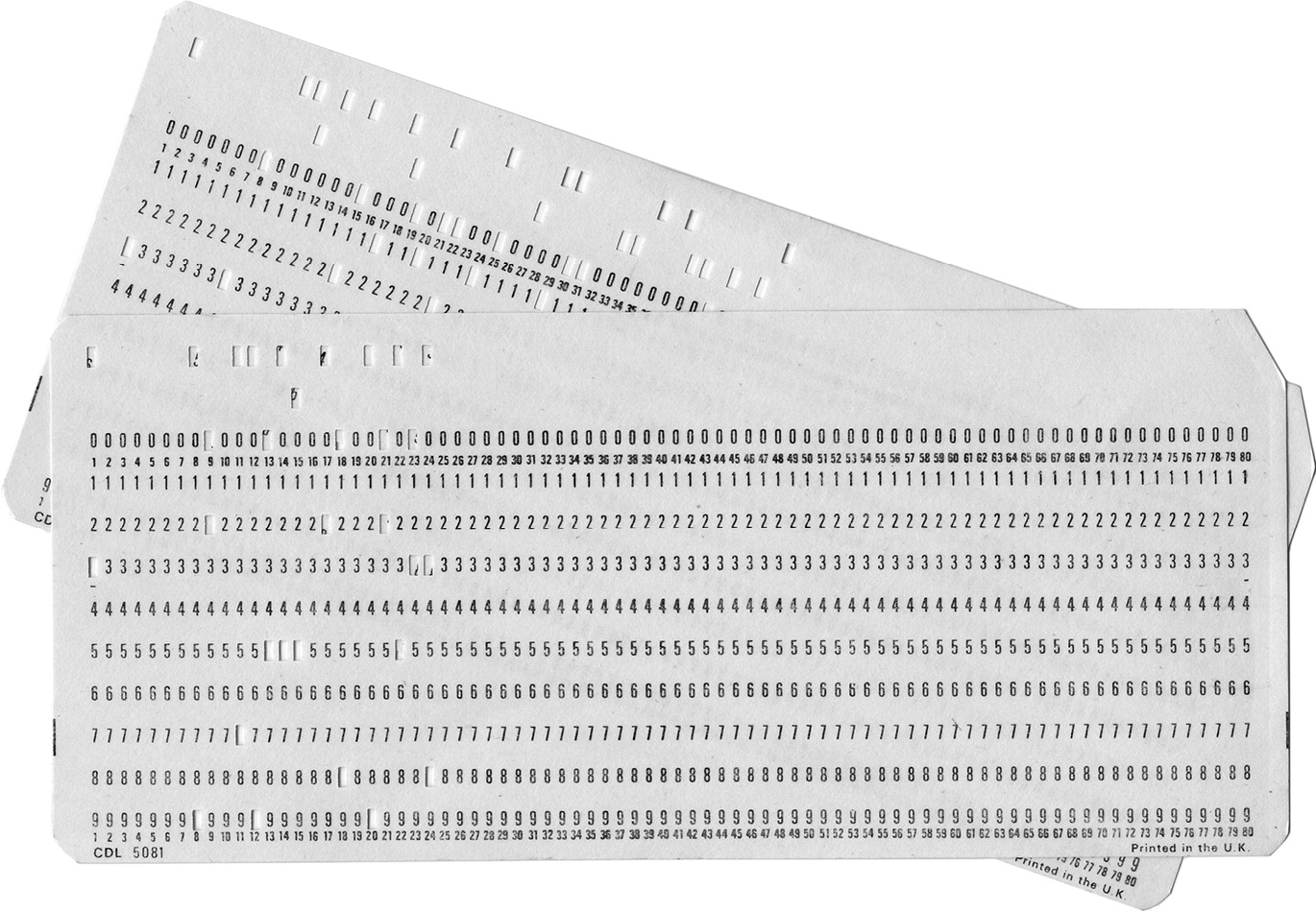
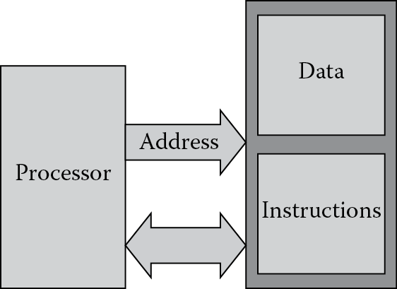
More definitions are probably in order before we start speaking of processors, programs, and bits. At the most fundamental level, we can look at machines that are given specific instructions or commands through any number of mechanisms—paper tape, switches, or magnetic materials. The machine certainly doesn’t have to be electronic to be considered. For example, in 1804 Joseph Marie Jacquard invented a way to weave designs into fabric by controlling the warp and weft threads on a silk loom with cards that had holes punched in them. Those same cards were actually modified (see Figure 1.7) and used in punch cards to feed instructions to electronic computers from the 1960s to the early 1980s. During the process of writing even short programs, these cards would fill up boxes, which were then handed to someone behind a counter with a card reader. Woe to the person who spent days writing a program using punch cards without numbering them, since a dropped box of cards, all of which looked nearly identical, would force someone to go back and punch a whole new set in the proper order! However the machine gets its instructions, to do any computational work those instructions need to be stored somewhere; otherwise, the user must reload them for each iteration. The stored-program computer, as it is called, fetches a sequence of instructions from memory, along with data to be used for performing calculations. In essence, there are really only a few components to a computer: a processor (something to do the actual work), memory (to hold its instructions and data), and busses to transfer the data and instructions back and forth between the two, as shown in Figure 1.8. Those instructions are the focus of this book—assembly language programming is the use of the most fundamental operations of the processor, written in a way that humans can work with them easily.
The classic model for a computer also shows typical interfaces for input/output (I/O) devices, such as a keyboard, a disk drive for storage, and maybe a printer. These interfaces connect to both the central processing unit (CPU) and the memory; however, embedded systems may not have any of these components! Consider a device such as an engine controller, which is still a computing system, only it has no human interfaces. The totality of the input comes from sensors that attach directly to the system-on-chip, and there is no need to provide information back to a video display or printer.
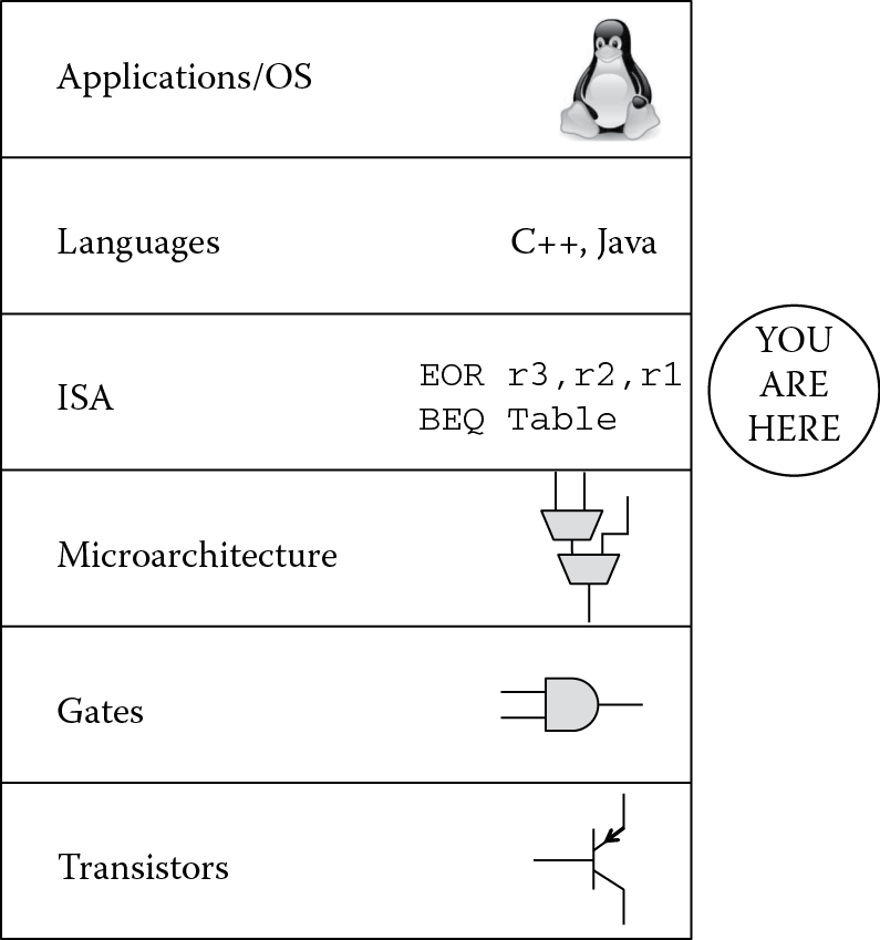
To get a better feel for where in the process of solving a problem we are, and to summarize the hierarchy of computing then, consider Figure 1.9. At the lowest level, you have transistors which are effectively moving electrons in a tightly controlled fashion to produce switches. These switches are used to build gates, such as AND, NOR and NAND gates, which by themselves are not particularly interesting. When gates are used to build blocks such as full adders, multipliers, and multiplexors, we can create a processor’s architecture, i.e., we can specify how we want data to be processed, how we want memory to be controlled, and how we want outside events such as interrupts to be handled. The processor then has a language of its own, which instructs various elements such as a multiplier to perform a task; for example, you might tell the machine to multiply two floating-point numbers together and store the result in a register. We will spend a great deal of time learning this language and seeing the best ways to write assembly code for the ARM architecture. Beyond the scope of what is addressed in this text, certainly you could go to the next levels, where assembly code is created from a higher-level language such as C or C++, and then on to work with operating systems like Android that run tasks or applications when needed.
1.4 Number Systems
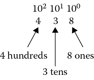
Since computers operate internally with transistors acting as switches, the combinational logic used to build adders, multipliers, dividers, etc., understands values of 1 or 0, either on or off. The binary number system, therefore, lends itself to use in computer systems more easily than base ten numbers. Numbers in base two are centered on the idea that each digit now represents a power of two, instead of a power of ten. In base ten, allowable numbers are 0 through 9, so if you were to count the number of sheep in a pasture, you would say 0, 1, 2, 3, 4, 5, 6, 7, 8, 9, and then run out of digits. Therefore, you place a 1 in the 10’s position (see Figure 1.10), to indicate you’ve counted this high already, and begin using the old digits again—10, 11, 12, 13, etc.
Now imagine that you only have two digits with which to count: 0 or 1. To count that same set of sheep, you would say 0, 1 and then you’re out of digits. We know the next value is 2 in base ten, but in base two, we place a 1 in the 2’s position and keep counting—10, 11, and again we’re out of digits to use. A marker is then placed in the 4’s position, and we do this as much as we like.
Example 1.1
Convert the binary number 1101012 to decimal.
Solution
This can be seen as
|
25 |
24 |
23 |
22 |
21 |
20 |
|
1 |
1 |
0 |
1 |
0 |
1 |
This would be equivalent to 32 + 16 + 4 + 1 = 5310.
The subscripts are normally only used when the base is not 10. You will see quickly that a number such as 101 normally doesn’t raise any questions until you start using computers. At first glance, this is interpreted as a base ten number—one hundred one. However, careless notation could have us looking at this number in base two, so be careful when writing and using numbers in different bases.
After staring at 1’s and 0’s all day, programming would probably have people jumping out of windows, so better choices for representing numbers are base eight (octal, although you’d be hard pressed to find a machine today that mainly uses octal notation) and base sixteen (hexadecimal or hex, the preferred choice), and here the digits are now a power of sixteen. These numbers pack quite a punch, and are surprisingly big when you convert them to decimal. Since counting in base ten permits the numbers 0 through 9 to indicate the number of 1’s, 10’s, 100’s, etc., in any given position, the numbers 0 through 9 don’t go far enough to indicate the number of 1’s we have in base sixteen. In other words, to count our sheep in base sixteen using only one digit, we would say 0, 1, 2, 3, 4, 5, 6, 7, 8, 9, and then we can keep going since the next position represents how many 16’s we have. So the first six letters of the alphabet are used as placeholders. So after 9, the counting continues—A, B, C, D, E, and then F. Once we’ve reached F, the next number is 1016.
Example 1.2
Find the decimal equivalent of A5E916.
Solution
This hexadecimal number can be viewed as
|
163 |
162 |
161 |
160 |
|
A |
5 |
E |
9 |
So our number above would be (10 × 163) + (5 × 162) + (14 × 161) + (9 × 160) = 42,47310. Notice that it’s easier to mentally treat the values A, B, C, D, E, and F as numbers in base ten when doing the conversion.
Example 1.3
Calculate the hexadecimal representation for the number 86210.
Solution
While nearly all handheld calculators today have a conversion function for this, it’s important that you can do this by hand (this is a very common task in programming). There are tables that help, but the easiest way is to simply evaluate how many times a given power of sixteen can go into your number. Since 163 is 4096, there will be none of these in your answer. Therefore, the next highest power is 162, which is 256, and there will be
862/256 = 3.3672
or 3 of them. This leaves
862 – (3 × 256) = 94.
The next highest power is 161, and this goes into 94 five times with a remainder of 14. Our number in hexadecimal is therefore
|
163 |
162 |
161 |
160 |
|
|
3 |
5 |
E |
The good news is that conversion between binary and hexadecimal is very easy—just group the binary digits, referred to as bits, into groups of four and convert the four digits into their hexadecimal equivalent. Table 1.1 shows the binary and hexadecimal values for decimal numbers from 0 to 15.
Binary and Hexadecimal Equivalents
|
Decimal |
Binary |
Hexadecimal |
|
0 |
0000 |
0 |
|
1 |
0001 |
1 |
|
2 |
0010 |
2 |
|
3 |
0011 |
3 |
|
4 |
0100 |
4 |
|
5 |
0101 |
5 |
|
6 |
0110 |
6 |
|
7 |
0111 |
7 |
|
8 |
1000 |
8 |
|
9 |
1001 |
9 |
|
10 |
1010 |
A |
|
11 |
1011 |
B |
|
12 |
1100 |
C |
|
13 |
1101 |
D |
|
14 |
1110 |
E |
|
15 |
1111 |
F |
Example 1.4
Convert the following binary number into hexadecimal:
110111110000101011112
Solution
By starting at the least significant bit (at the far right) and grouping four bits together at a time, the first digit would be F16, as shown below.
The second group of four bits would then be 10102 or A16, etc., giving us
DF0AF16.
One comment about notation—you might see hexadecimal numbers displayed as 0xFFEE or &FFEE (depending on what’s allowed by the software development tools you are using), and binary numbers displayed as 2_1101 or b1101.
1.5 Representations of Numbers and Characters
All numbers and characters are simply bit patterns to a computer. It’s unfortunate that something inside microprocessors cannot interpret a programmer’s meaning, since this could have saved countless hours of debugging and billions of dollars in equipment. Programmers have been known to be the cause of lost space probes, mostly because the processor did exactly what the software told it to do. When you say 0x6E, the machine sees 0x6E, and that’s about it. This could be a character (a lowercase “n”), the number 110 in base ten, or even a fractional value! We’re going to come back to this idea over and over—computers have to be told how to treat all types of data. The programmer is ultimately responsible for interpreting the results that a processor provides and making it clear in the code. In these next three sections, we’ll examine ways to represent integer numbers, floating-point numbers, and characters, and then see another way to represent fractions in Chapter 7.
1.5.1 Integer Representations
For basic mathematical operations, it’s not only important to be able to represent numbers accurately but also use as few bits as possible, since memory would be wasted to include redundant or unnecessary bits. Integers are often represented in byte (8-bit), halfword (16-bit), and word (32-bit) quantities. They can be longer depending on their use, e.g., a cryptography routine may require 128-bit integers.
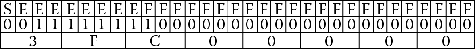
Unsigned representations make the assumption that every bit signifies a positive contribution to the value of the number. For example, if the hexadecimal number 0xFE000004 were held in a register or in memory, and assuming we treat this as an unsigned number, it would have the decimal value
(15 × 167) + (14 × 166) + (4 × 160) = 4,261,412,868.
Signed representations make the assumption that the most significant bit is used to create positive and negative values, and they come in three flavors: sign-magnitude, one’s complement and two’s complement.
Sign-magnitude is the easiest to understand, where the most significant bit in the number represents a sign bit and all other bits represent the magnitude of the number. A one in the sign bit indicates the number is negative and a zero indicates it is positive.
Example 1.5
The numbers −18 and 25 are represented in 16 bits as
–18 = 1000000000010010
25 = 0000000000011001
To add these two numbers, it’s first necessary to determine which number has the larger magnitude, and then the smaller number would be subtracted from it. The sign would be the sign of the larger number, in this case a zero. Fortunately, sign-magnitude representations are not used that much, mostly because their use implies making comparisons first, and this adds extra instructions in code just to perform basic math.
One’s complement numbers are not used much in modern computing systems either, mostly because there is too much extra work necessary to perform basic arithmetic operations. To create a negative value in this representation, simply invert all the bits of its positive, binary value. The sign bit will be a 1, just like sign-magnitude representations, but there are two issues that arise when working with these numbers. The first is that you end up with two representations for 0, and the second is that it may be necessary to adjust a sum when adding two values together, causing extra work for the processor. Consider the following two examples.
Example 1.6
Assuming that you have 16 bits to represent a number, add the values −124 to 236 in one’s complement notation.
Solution
To create −124 in one’s complement, simply write out the binary representation for 124, and then invert all the bits:
124 0000000001111100
–124 1111111110000011
Adding 236 gives us
The problem is that the answer is actually 112, or 0x70 in hex. In one’s complement notation, a carry in the most significant bit forces us to add a one back into the sum, which is one extra step:
Example 1.7
Add the values −8 and 8 together in one’s complement, assuming 8 bits are available to represent the numbers.
Solution
Again, simply take the binary representation of the positive value and invert all the bits to get −8:
Since there was no carry from the most significant bit, this means that 00000000 and 11111111 both represent zero. Having a +0 and a –0 means extra work for software, especially if you’re testing for a zero result, leading us to the use of two’s complement representations and avoiding this whole problem.
Two’s complement representations are easier to work with, but it’s important to interpret them correctly. As with the other two signed representations, the most significant bit represents the sign bit. However, in two’s complement, the most significant bit is weighted, which means that it has the same magnitude as if the bit were in an unsigned representation. For example, if you have 8 bits to represent an unsigned number, then the most significant bit would have the value of 27, or 128. If you have 8 bits to represent a two’s complement number, then the most significant bit represents the value −128. A base ten number n can be represented as an m-bit two’s complement number, with b being an individual bit’s value, as
To interpret this more simply, the most significant bit can be thought of as the only negative component to the number, and all the other bits represent positive components. As an example, −114 represented as an 8-bit, two’s complement number is
100011102 = –27 + 23 + 22 + 21 = –114.
Notice in the above calculation that the only negative value was the most significant bit. Make no mistake—you must be told in advance that this number is treated as a two’s complement number; otherwise, it could just be the number 142 in decimal.
The two’s complement representation provides a range of positive and negative values for a given number of bits. For example, the number 8 could not be represented in only 4 bits, since 10002 sets the most significant bit, and the value is now interpreted as a negative number (–8, in this case). Table 1.2 shows the range of values produced for certain bit lengths, using ARM definitions for halfword, word, and double word lengths.
Two’s Complement Integer Ranges
|
Length |
Number of Bits |
Range |
|
m |
–2m –1 to 2m −1–1 |
|
|
Byte |
8 |
–128 to 127 |
|
Halfword |
16 |
–32,768 to 32,767 |
|
Word |
32 |
–2,147,483,648 to 2,147,483,647 |
|
Double word |
64 |
–264 to 264 –1 |
Note : To calculate the two’s complement representation of a negative number, simply take its magnitude, convert it to binary, invert all the bits, and then add 1.
Example 1.8
Convert −9 to a two’s complement representation in 8 bits.
Solution
Since 9 is 10012, the 8-bit representation of −9 would be
Arithmetic operations now work as expected, without having to adjust any final values. To convert a two’s complement binary number back into decimal, you can either subtract one and then invert all the bits, which in this case is the fastest way, or you can view it as –27 plus the sum of the remaining weighted bit values, i.e.,
–27 + 26 + 25 + 24 + 22 + 21 + 20 =
–128 + 119 =
–9
Example 1.9
Add the value −384 to 2903 using 16-bit, two’s complement arithmetic.
Solution
First, convert the two values to their two’s complement representations:
1.5.2 Floating-Point Representations
In many applications, values larger than 2,147,483,647 may be needed, but you still have only 32 bits to represent numbers. Very large and very small values can be constructed by using a floating-point representation. While the format itself has a long history to it, with many varieties of it appearing in computers over the years, the IEEE 754 specification of 1985 (Standards Committee 1985) formally defined a 32-bit data type called single-precision, which we’ll cover extensively in Chapter 9. These floating-point numbers consist of an exponent, a fraction, a sign bit, and a bias. For “normal” numbers, and here “normal” is defined in the specification, the value of a single-precision number F is given as
F = –1s × 1.f × 2e−b
where s is the sign bit, and f is the fraction made up of the lower 23 bits of the format. The most significant fraction bit has the value 0.5, the next bit has the value 0.25, and so on. To ensure all exponents are positive numbers, a bias b is added to the exponent e. For single-precision numbers, the exponent bias is 127.
While the range of an unsigned, 32-bit integer is 0 to 232-1 (4.3 × 10⁹), the positive range of a single-precision floating-point number, also represented in 32 bits, is 1.2 × 10−38 to 3.4 × 10+38! Note that this is only the positive range; the negative range is congruent. The amazing range is a trade-off, actually. Floating-point numbers trade accuracy for range, since the delta between representable numbers gets larger as the exponent gets larger. Integer formats have a fixed precision (each increment is equal to a fixed value).
Example 1.10
Represent the number 1.5 in a single-precision, floating-point format.
We would form the value as
s = 0 (a positive number)
f = 100 0000 0000 0000 0000 0000 (23 fraction bits representing 0.5)
e = 0 + 127 (8 bits of true exponent plus the bias)
F = 0 0111111 100 0000 0000 0000 0000 0000
or 0x3FC00000, as shown in Figure 1.11.
The large dynamic range of floating-point representations has made it popular for scientific and engineering computing. While we’ve only seen the single-precision format, the IEEE 754 standard also specifies a 64-bit, double-precision format that has a range of ±2.2 × 10−308 to 1.8 × 10+308! Table 1.3 shows what two of the most common formats specified in the IEEE standard look like (single- and double-precision). Single precision provides typically 6–9 digits of numerical precision, while double precision gives 15–17.
IEEE 754 Single- and Double-Precision Formats
|
Format |
Single Precision |
Double Precision |
|
Format width in bits |
32 |
64 |
|
Exponent width in bits |
8 |
11 |
|
Fraction bits |
23 |
52 |
|
Exp maximum |
+127 |
+1023 |
|
Exp minimum |
–126 |
–1022 |
|
Exponent bias |
127 |
1023 |
Special hardware is required to handle numbers in these formats. Historically, floating-point units were separate ICs that were attached to the main processor, e.g., the Intel 80387 for the 80386 and the Motorola 68881 for the 68000. Eventually these were integrated onto the same die as the processor, but at a cost. Floating-point units are often quite large, typically as large as the rest of the processor without caches and other memories. In most applications, floating-point computations are rare and not speed-critical. For these reasons, most microcontrollers do not include specialized floating-point hardware; instead, they use software routines to emulate floating-point operations. There is actually another format that can be used when working with real values, which is a fixed-point format; it doesn’t require a special block of hardware to implement, but it does require careful programming practices and often complicated error and bounds analysis. Fixed-point formats will be covered in great detail in Chapter 7.
1.5.3 Character Representations
Bit patterns can represent numbers or characters, and the interpretation is based entirely on context. For example, the binary pattern 01000001 could be the number 65 in an audio codec routine, or it could be the letter “A”. The program determines how the pattern is used and interpreted. Fortunately, standards for encoding character data were established long ago, such as the American Standard Code for Information Interchange, or ASCII, where each letter or control character is mapped to a binary value. Other standards include the Extended Binary-Coded-Decimal Interchange Code (EBCDIC) and Baudot, but the most commonly used today is ASCII. The ASCII table for character codes can be found in Appendix C.
While most devices may only need the basic characters, such as letters, numbers, and punctuation marks, there are some control characters that can be interpreted by the device. For example, old teletype machines used to have a bell that rang in a Pavlovian fashion, alerting the user that something exciting was about to happen. The control character to ring the bell is 0x07. Other control characters include a backspace (0x08), a carriage return (0x0D), a line feed (0x0A), and a delete character (0x7F), all of which are still commonly used.
Using character data in assembly language is not difficult, and most assemblers will let you use a character in the program without having to look up the equivalent hexadecimal value in a table. For example, instead of saying
MOV r0, #0x42; move a ‘B’ into register r0
you can simply say
MOV r0, #’B’; move a ‘B’ into register r0
Character data will be seen throughout the book, so it’s worth spending a little time becoming familiar with the hexadecimal equivalents of the alphabet.
1.6 Translating Bits to Commands
All processors are programmed with a set of instructions, which are unique patterns of bits, or 1’s and 0’s. Each set is unique to that particular processor. These instructions might tell the processor to add two numbers together, move data from one place to another, or sit quietly until something wakes it up, like a key being pressed. A processor from Intel, such as the Pentium 4, has a set of bit patterns that are completely different from a SPARC processor or an ARM926EJ-S processor. However, all instruction sets have some common operations, and learning one instruction set will help you understand nearly any of them.
The instructions themselves can be of different lengths, depending on the processor architecture—8, 16, or 32 bits long, or even a combination of these. For our studies, the instructions are either 16 or 32 bits long; although, much later on, we’ll examine how the ARM processors can use some shorter, 16-bit instructions in combination with 32-bit Thumb-2 instructions. Reading and writing a string of 1’s and 0’s can give you a headache rather quickly, so to aid in programming, a particular bit pattern is mapped onto an instruction name, or a mnemonic, so that instead of reading
E0CC31B0
1AFFFFF1
E3A0D008
the programmer can read
STRH sum, [pointer], #16
BNE loop_one
MOV count, #8
which makes a little more sense, once you become familiar with the instructions themselves.
Example 1.11
Consider the bit pattern for the instruction above:
MOV count, #8
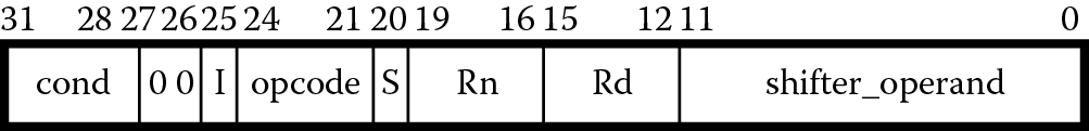
The pattern is the hex number 0xE3A0D008. From Figure 1.12, you can see that the ARM processor expects parts of our instruction in certain fields—the number 8, for example, would be placed in the field called 8_bit_immediate, and the instruction itself, moving a number into a register, is encoded in the field called opcode. The parameter called count is a convenience that allows the programmer to use names instead of register numbers. So somewhere in our program, count is assigned to a real register and that register number is encoded into the field called Rd. We will see the uses of MOV again in Chapter 6.
Most mnemonics are just a few letters long, such as B for branch or ADD for, well, add. Microprocessor designers usually try and make the mnemonics as clear as possible, but every once in a while you come across something like RSCNE (from ARM), DCBZ (from IBM) or the really unpronounceable AOBLSS (from DEC) and you just have to look it up. Despite the occasionally obtuse name, it is still much easier to remember RSCNE than its binary or hex equivalent, as it would make programming nearly impossible if you had to remember each command’s pattern. We could do this mapping or translation by hand, taking the individual mnemonics, looking them up in a table, then writing out the corresponding bit pattern of 1’s and 0’s, but this would take hours, and the likelihood of an error is very high. Therefore, we rely on tools to do this mapping for us.
To complicate matters, reading assembly language commands is not always trivial, even for advanced programmers. Consider the sequence of mnemonics for the IA-32 architecture from Intel:
mov eax, DWORD PTR _c
add eax, DWORD PTR _b
mov DWORD PTR _a, eax
cmp DWORD PTR _a, 4
This is actually seen as pretty typical code, really—not so exotic. Even more intimidating to a new learner, mnemonics for the ColdFire microprocessor look like this:
mov.l (0,%a2,%d2.l*4),%d6
mac.w %d6:u,%d5:u <<1
mac.w %d6:l,%d3:u <<1
Where an experienced programmer would immediately recognize these commands as just variations on basic operations, along with extra characters to make the software tools happy, someone just learning assembly would probably close the book and go home. The message here is that coding in assembly language takes practice and time to learn. Each processor’s instruction set looks different, and tools sometimes force a few changes to the syntax, producing something like the above code; however, nearly all assembly formats follow some basic rules. We will begin learning assembly using ARM instructions, which are very readable.
1.7 The Tools
At some point in the history of computing, it became easier to work with high-level languages instead of coding in 1’s and 0’s, or machine code, and programmers described loops and variables using statements and symbols. The earlier languages include COBOL, FORTRAN, ALGOL, Forth, and Ada. FORTRAN was required knowledge for an undergraduate electrical engineering student in the 1970s and 1980s, and that has largely been replaced with C, C++, Java, and even Python. All of these languages still have one thing in common: they all contain near-English descriptions of code that are then translated into the native instruction set of the microprocessor. The program that does this translation is called a compiler, and while compilers get more and more sophisticated, their basic purpose remains the same, taking something like an “if…then” statement and converting it into assembly language. Modern systems are programmed in high-level languages much of the time to allow code portability and to reduce design time.
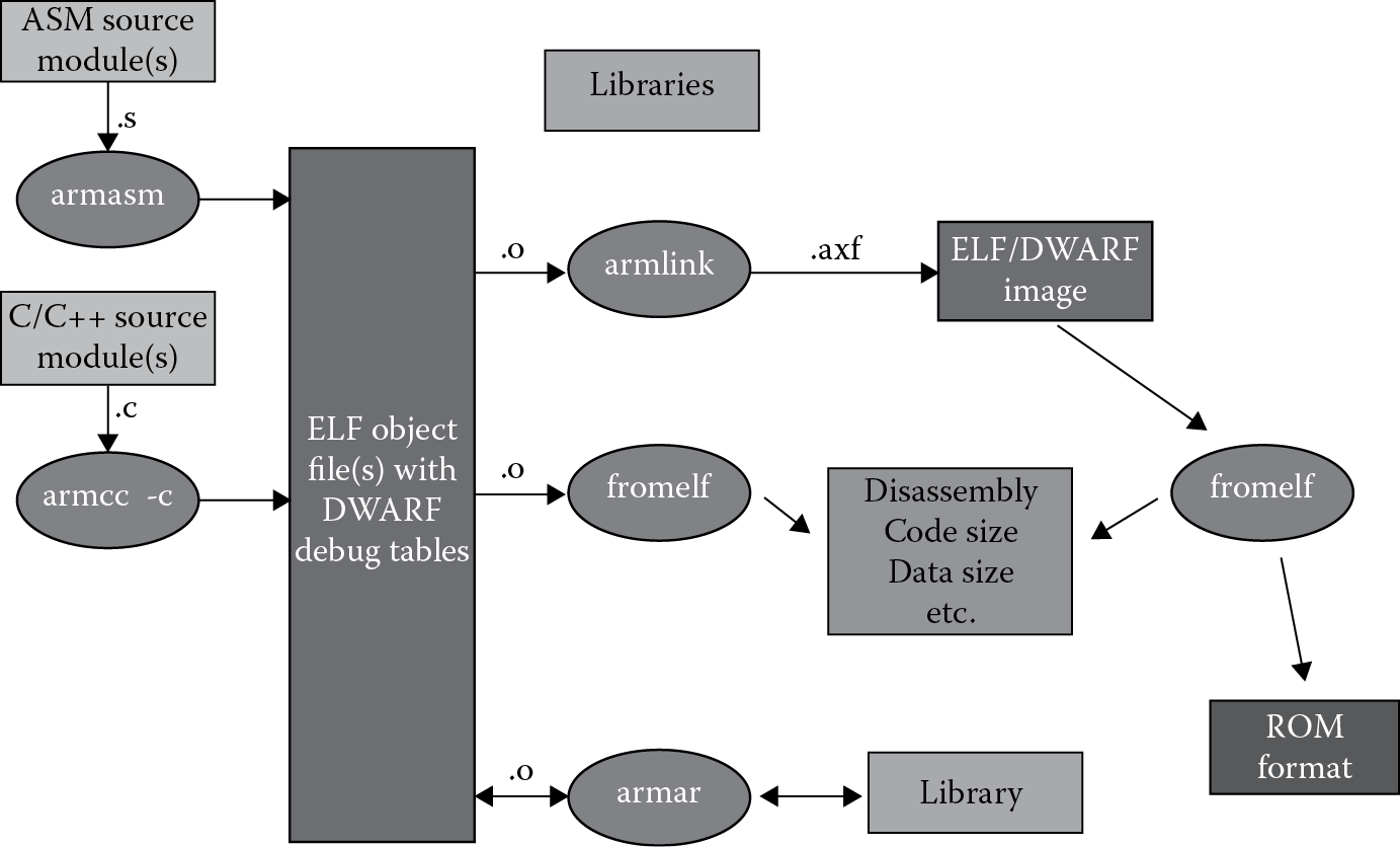
As with most programming tasks, we also need an automated way of translating our assembly language instructions into bit patterns, and this is precisely what an assembler does, producing a file that a piece of hardware (or a software simulator) can understand, in machine code using only 1’s and 0’s. To help out even further, we can give the assembler some pseudo-instructions, or directives (either in the code or with options in the tools), that tell it how to do its job, provided that we follow the particular assembler’s rules such as spacing, syntax, the use of certain markers like commas, etc. If you follow the tools flow in Figure 1.13, you can see that an object file is produced by the assembler from our source file, or the file that contains our assembly language program. Note that a compiler will also use a source file, but the code might be C or C++. Object files differ from executable files in that they often contain debugging information, such as program symbols (names of variables and functions) for linking or debugging, and are usually used to build a larger executable. Object files, which can be produced in different formats, also contain relocation information. Once you’ve assembled your source files, a linker can then be used to combine them into an executable program, even including other object files, say from customized libraries. Under test conditions, you might choose to run these files in a debugger (as we’ll do for the majority of examples), but usually these executables are run by hardware in the final embedded application. The debugger provides access to registers on the chip, views of memory, and the ability to set and clear breakpoints and watchpoints, which are methods of stopping the processor on instruction or memory accesses, respectively. It also provides views of code in both high-level languages and assembly.
1.7.1 Open Source Tools
Many students and professors steer clear of commercial software simply to avoid licensing issues; most software companies don’t make it a policy to give away their tools, but there are non-profits that do provide free toolchains. Linaro, a not-for-profit engineering organization, focuses on optimizing open source software for the ARM architecture, including the GCC toolchain and the Linux kernel, and providing regular releases of the various tools and operating systems. You can find downloads on their website (www.linaro.org). What they define as “bare-metal” builds for the tools can also be found if you intend on working with gcc (the gnu compiler) and gdb (the gnu debugger). Clicking on the links take you to prebuilt gnu toolchains for Cortex-M and Cortex-R controllers located at https://launchpad.net/gcc-arm-embedded. There are dozens of other open source sites for ARM tools, found with a quick Web search.
1.7.2 Keil (ARM)
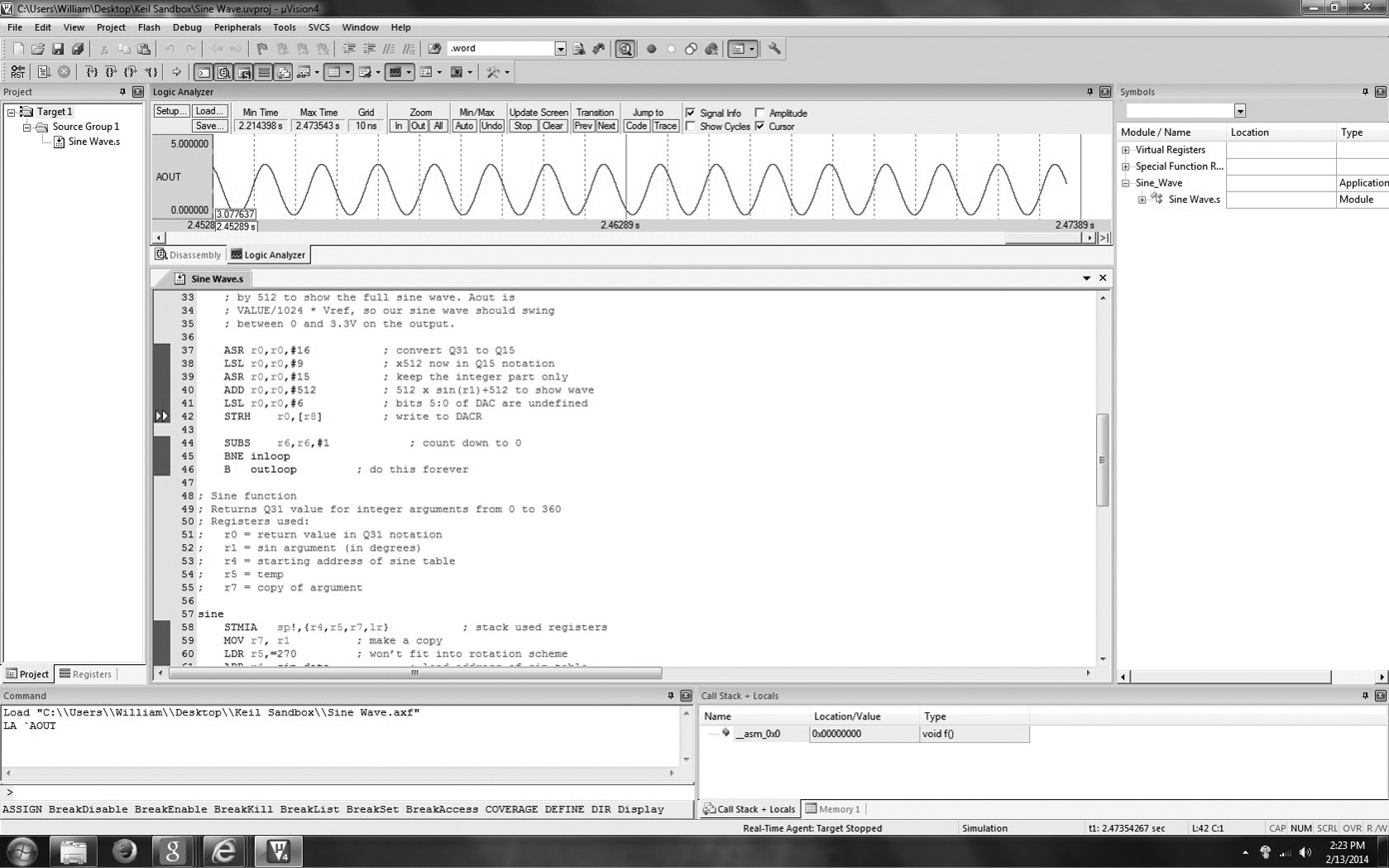
ARM’s C and C++ compilers generate optimized code for all of the instruction sets, ARM, Thumb, and Thumb-2, and support full ISO standard C and C++. Modern tool sets, like ARM’s RealView Microcontroller Development Kit (RVMDK), which is found at http://www.keil.com/demo, can display both the high-level code and its assembly language equivalent together on the screen, as shown in Figure 1.14. Students have found that the Keil tools are relatively easy to use, and they support hundreds of popular microcontrollers. A limitation appears when a larger microprocessor, such as a Cortex-A9, is used in a project, since the Keil tools are designed specifically for microcontrollers. Otherwise, the tools provide everything that is needed:
- C and C++ compilers
- Macro assembler
- Linker
- True integrated source-level debugger with a high-speed CPU and peripheral simulator for popular ARM-based microcontrollers
- µVision4 Integrated Development Environment (IDE), which includes a full-featured source code editor, a project manager for creating and maintaining projects, and an integrated make facility for assembling, compiling, and linking embedded applications
- Execution profiler and performance analyzer
- File conversion utility (to convert an executable file to a HEX file, for example)
- Links to development tools manuals, device datasheets, and user’s guides
It turns out that you don’t always choose either a high-level language or assembly language for a particular project—sometimes, you do both. Before you progress through the book, read the Getting Started User’s Guide in the RVMDK tools’ documentation.
1.7.3 Code Composer Studio
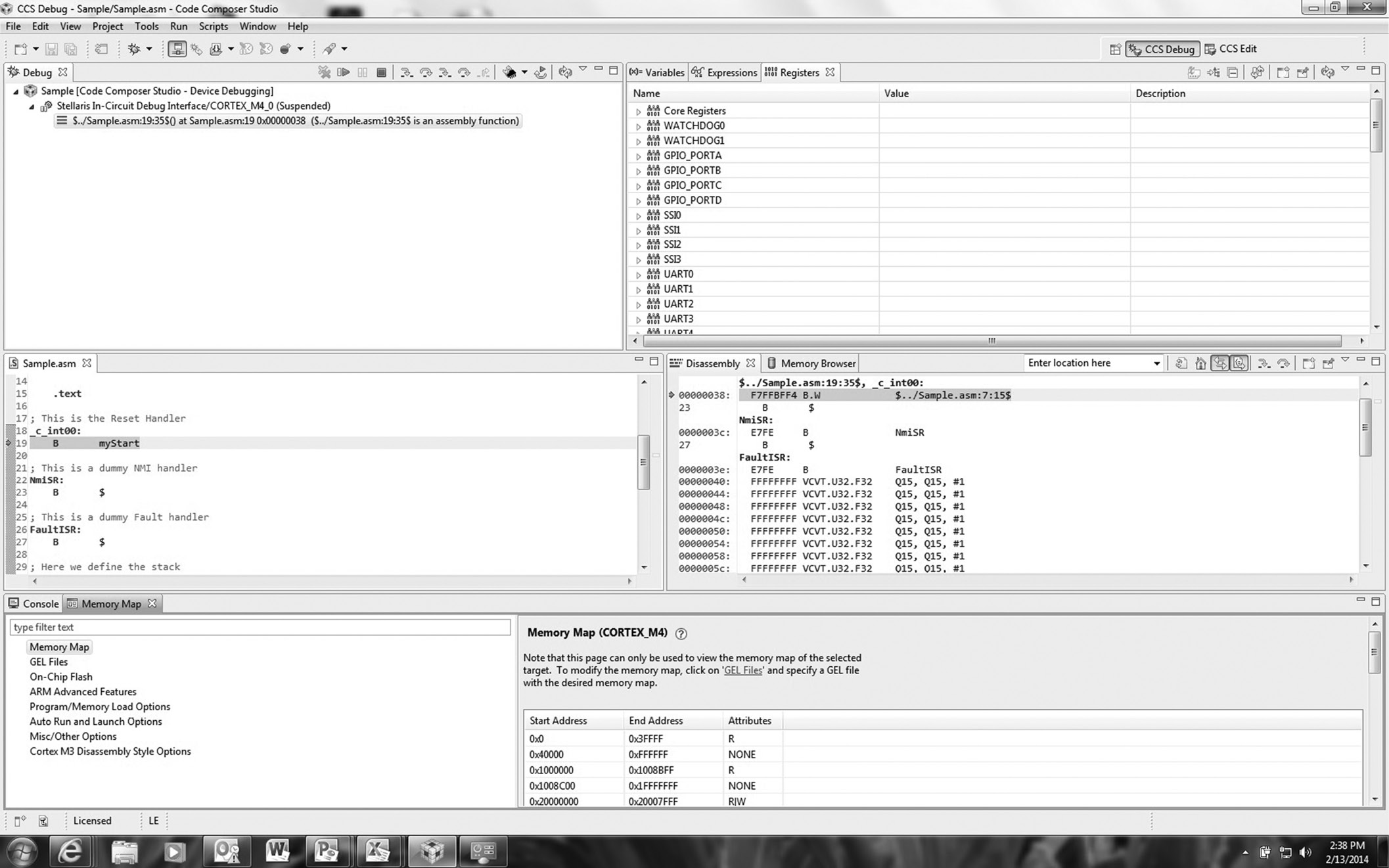
Texas Instruments has a long history of building ARM-based products, and as a leading supplier, makes their own tools. Code Composer Studio (CCS) actually supports all of their product lines, not just ARM processors. As a result, they include some rather nice features, such as a free operating system (SYS/BIOS), in their tool suite. The CCS tools support microcontrollers, e.g., the Cortex-M4 products, as well as very large SoCs like those in their Davinci and Sitara lines, so there is some advantage in starting with a more comprehensive software package, provided that you are aware of the learning curve associated with it. The front end to the tools is based on the Eclipse open source software framework, shown in Figure 1.15, so if you have used another development tool for Java or C++ based on Eclipse, the CCS tools might look familiar. Briefly, the CCS tools include:
- Compilers for each of TI’s device families
- Source code editor
- Project build environment
- Debugger
- Code profiler
- Simulators
- A real-time operating system
Appendix A provides step-by-step instructions for running a small assembly program in CCS—it’s highly unorthodox and not something done in industry, but it’s simple and it works!
1.7.4 Useful Documentation
The following free documents are likely to be used often for looking at formats, examples, and instruction details:
- ARM Ltd. 2009. Cortex-M4 Technical Reference Manual. Doc. no. DDI0439C (ID070610). Cambridge: ARM Ltd.
- ARM Ltd. 2010. ARM v7-M Architectural Reference Manual. Doc. no. DDI0403D. Cambridge: ARM Ltd.
- Texas Instruments. 2012. ARM Assembly Language Tools v5.0 User’s Guide. Doc. no. SPNU118K. Dallas: Texas Instruments.
- ARM Ltd. 2012. RealView Assembler User Guide (online), Revision D. Cambridge: ARM Ltd.
1.8 Exercises
- Give two examples of system-on-chip designs available from semiconductor manufacturers. Describe their features and interfaces. They do not necessarily have to contain an ARM processor.
- Find the two’s complement representation for the following numbers, assuming they are represented as a 16-bit number. Write the value in both binary and hexadecimal.
- –93
- 1034
- 492
- –1094
- Convert the following binary values into hexadecimal:
- 10001010101111
- 10101110000110
- 1011101010111110
- 1111101011001110
- Write the 8-bit representation of –14 in one’s complement, two’s complement, and sign-magnitude representations.
- Convert the following hexadecimal values to base ten:
- 0xFE98
- 0xFEED
- 0xB00
- 0xDEAF
- Convert the following base ten numbers to base four:
- 812
- 101
- 96
- 3640
- Using the smallest data size possible, either a byte, a halfword (16 bits), or a word (32 bits), convert the following values into two’s complement representations:
- –18,304
- –20
- 114
- –128
- Indicate whether each value could be represented by a byte, a halfword, or a word-length two’s complement representation:
- –32,765
- 254
- –1,000,000
- –128
- Using the information from the ARM v7-M Architectural Reference Manual, write out the 16-bit binary value for the instruction SMULBB r5, r4, r3.
- Describe all the ways of interpreting the hexadecimal number 0xE1A02081 (hint: it might not be data).
- If the hexadecimal value 0xFFE3 is a two’s complement, halfword value, what would it be in base ten? What if it were a word-length value (i.e., 32 bits long)?
- How do you think you could quickly compute values in octal (base eight) given a value in binary?
- Convert the following decimal numbers into hexadecimal:
- 256
- 1000
- 4095
- 42
- Write the 32-bit representation of –247 in sign-magnitude, one’s complement, and two’s complement notations. Write the answer using 8 hex digits.
- Write the binary pattern for the letter “Q” using the ASCII representation.
- Multiply the following binary values. Notice that binary multiplication works exactly like decimal multiplication, except you are either adding 0 to the final product or a scaled multiplicand. For example:
- How many bits would the following C data types use by the ARM7TDMI?
- int
- long
- char
- short
- long long
- Write the decimal number 1.75 in the IEEE single-precision floating-point format. Use one of the tools given in the References to check your answer.