Table of Contents for
Modern Assembly Language Programming with the ARM Processor
 Modern Assembly Language Programming with the ARM Processor
Published by
Newnes, 2016
Modern Assembly Language Programming with the ARM Processor
Published by
Newnes, 2016
- Modern Assembly Language Programming with the ARM Processor
- Cover image
- Title page
- Table of Contents
- Copyright
- List of Tables
- List of Figures
- List of Listings
- Preface
- Companion Website
- Acknowledgments
- Part I: Assembly as a Language
- Chapter 1: Introduction
- Chapter 2: GNU Assembly Syntax
- Chapter 3: Load/Store and Branch Instructions
- Chapter 4: Data Processing and Other Instructions
- Chapter 5: Structured Programming
- Chapter 6: Abstract Data Types
- Part II: Performance Mathematics
- Chapter 7: Integer Mathematics
- Chapter 8: Non-Integral Mathematics
- Chapter 9: The ARM Vector Floating Point Coprocessor
- Chapter 10: The ARM NEON Extensions
- 10.10 Multiplication and Division
- Part III: Accessing Devices
- Chapter 11: Devices
- Chapter 12: Pulse Modulation
- Chapter 13: Common System Devices
- Chapter 14: Running Without an Operating System
- Index
Common System Devices
Abstract
This chapter briefly describes some of the devices which are present in most modern computer systems. It then describes in detail the clock management devices on the Raspberry Pi and the pcDuino. Next, it gives an explanation of asynchronous serial communications, and explains how there is some tolerance for mismatch between the clock rate of the transmitter and receiver. It then explains the Universal Asynchronous Receiver/Transmitter (UART) device. Next it covers in detail the UART devices present on the Raspberry Pi and the PcDuino. Once again, the reader is given the opportunity to do a comparison between two different devices which perform almost precisely the same functions.
Keywords
Universal asynchronous receiver/transmitter (UART); Clock manager; Serial communications; RS232
There are some classes of devices that are found in almost every system, including the smallest embedded systems. Such common devices include hardware for managing the clock signals sent to other devices, and serial communications (typically RS232). Most mid-sized or large systems also include devices for managing virtual memory, managing the cache, driving a display, interfacing with keyboard and mouse, accessing disk and other storage devices, and networking. Small embedded systems may have devices for converting analog signals to digital and vice versa, pulse width modulation, and other purposes. Some systems, such as the Raspberry Pi and pcDuino, have all or most of the devices of large systems, as well as most of the devices found on embedded systems. In this chapter, we look at two devices found on almost every system.
13.1 Clock Management Device
Very simple computer systems can be driven by a single clock. Most devices, including the CPU, are designed as state machines. The clock device sends a square-wave signal at a fixed frequency to all devices that need it. The clock signal tells the devices when to transition to the next state. Without the clock signal, none of the devices would do anything.
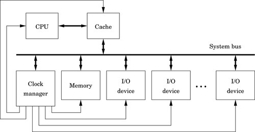
More complex computers may contain devices which need to run at different rates. This requires the system to have separate clock signals for each device (or group of devices). System designers often solve this problem by adding a clock manager device to the system. This device allows the programmer to configure the clock signals that are sent to the other devices in the system. Fig. 13.1 shows a typical system. The clock manager, just like any other device, is configured by the CPU writing data to its registers using the system bus.
13.1.1 Raspberry Pi Clock Manager
The BCM2835 system-on-chip contains an ARM CPU and several devices. Some of the devices need their own clock to drive their operation at the correct frequency. Some devices, such as serial communications receivers and transmitters, need configurable clocks so that the programmer has control over the speed of the device. To provide this flexibility and allow the programmer to have control over the clocks for each device, the BCM2835 includes a clock manager device, which can be used to configure the clock signals driving the other devices in the system.
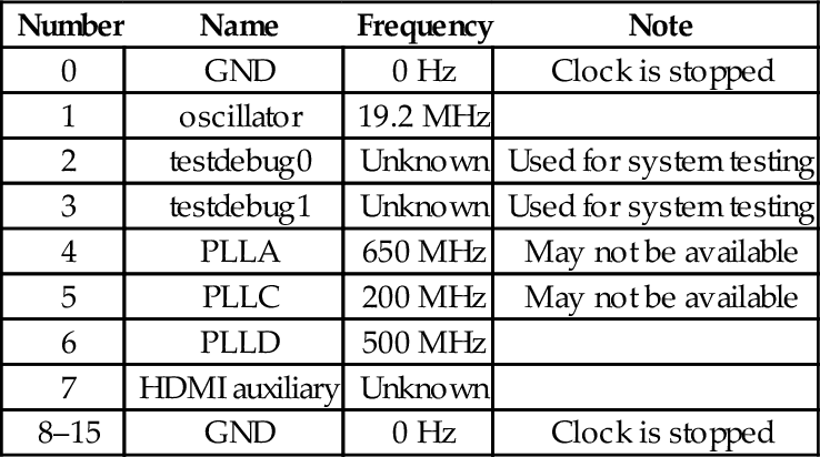
The Raspberry Pi has a 19.2 MHz oscillator which can be used as a base frequency for any of the clocks. The BCM2835 also has three phase-locked-loop circuits that boost the oscillator to higher frequencies. Table 13.1 shows the frequencies that are available from various sources. Each device clock can be driven by one of the PLLs, the external 19.2 MHz oscillator, a signal from the HDMI port, or either of two test/debug inputs.
Table 13.1
Clock sources available for the clocks provided by the clock manager
| Number | Name | Frequency | Note |
| 0 | GND | 0 Hz | Clock is stopped |
| 1 | oscillator | 19.2 MHz | |
| 2 | testdebug0 | Unknown | Used for system testing |
| 3 | testdebug1 | Unknown | Used for system testing |
| 4 | PLLA | 650 MHz | May not be available |
| 5 | PLLC | 200 MHz | May not be available |
| 6 | PLLD | 500 MHz | |
| 7 | HDMI auxiliary | Unknown | |
| 8–15 | GND | 0 Hz | Clock is stopped |
Among the clocks controlled by the clock manager device are the core clock (CM_VPU), the system timer clock (PM_TIME) which controls the speed of the system timer, the GPIO clocks which are documented in the Raspberry Pi peripheral documentation, the pulse modulator device clocks, and the serial communications clocks. It is generally not a good idea to modify the settings of any of the clocks without good reason.
The base address of the clock manager device is 2010100016. Some of the clock manager registers are shown in Table 13.2. Each clock is managed by two registers: a control register and a divisor. The control register is used to enable or disable a clock, to select which source oscillator drives the clock, and to select an optional multistage noise shaping (MASH) filter level. MASH filtering is useful for reducing the perceived noise when a clock is being used to generate an audio signal. In most cases, MASH filtering should not be used.
Table 13.2
Some registers in the clock manager device
| Offset | Name | Description |
| 07016 | CM_GP0_CTL | GPIO Clock 0 (GPCLK0) Control |
| 07416 | CM_GP0_DIV | GPIO Clock 0 (GPCLK0) Divisor |
| 07816 | CM_GP1_CTL | GPIO Clock 1 (GPCLK1) Control |
| 07c16 | CM_GP1_DIV | GPIO Clock 1 (GPCLK1) Divisor |
| 08016 | CM_GP2_CTL | GPIO Clock 2 (GPCLK2) Control |
| 08416 | CM_GP2_DIV | GPIO Clock 2 (GPCLK2) Divisor |
| 09816 | CM_PCM_CTL | Pulse Code Modulator Clock (PCM_CLK) Control |
| 09c16 | CM_PCM_DIV | Pulse Code Modulator Clock (PCM_CLK) Divisor |
| 0a016 | CM_PWM_CTL | Pulse Modulator Device Clock (PWM_CLK) Control |
| 0a416 | CM_PWM_DIV | Pulse Modulator Device Clock (PWM_CLK) Divisor |
| 0f016 | CM_UART_CTL | Serial Communications Clock (UART_CLK) Control |
| 0f416 | CM_UART_DIV | Serial Communications Clock (UART_CLK) Divisor |
Table 13.3 shows the meaning of the bits in the control registers for each of the clocks, and Table 13.4 shows the fields in the clock manager divisor registers. The procedure for configuring one of the clocks is:
Table 13.3
Bit fields in the clock manager control registers
| Bit | Name | Description |
| 3–0 | SRC | Clock source chosen from Table 13.1 |
| 4 | ENAB | Writing a 0 causes the clock to shut down. The clock will not stop immediately. The BUSY bit will be 1 while the clock is shutting down. When the BUSY bit becomes 0, the clock has stopped and it is safe to reconfigure it. Writing a 1 to this bit causes the clock to start |
| 5 | KILL | Writing a 1 to this bit will stop and reset the clock. This does not shut down the clock cleanly, and could cause a glitch in the clock output |
| 6 | - | Unused |
| 7 | BUSY | A 1 in this bit indicates that the clock is running |
| 8 | FLIP | Writing a 1 to this bit will invert the clock output. Do not change this bit while the clock is running |
| 10–9 | MASH | Controls how the clock source is divided.
01: 1-stage MASH division 10: 2-stage MASH division 11: 3-stage MASH division Do not change this while the clock is running. |
| 23–11 | – | Unused |
| 31–24 | PASSWD | This field must be set to 5A16 every time the clock control register is written to |
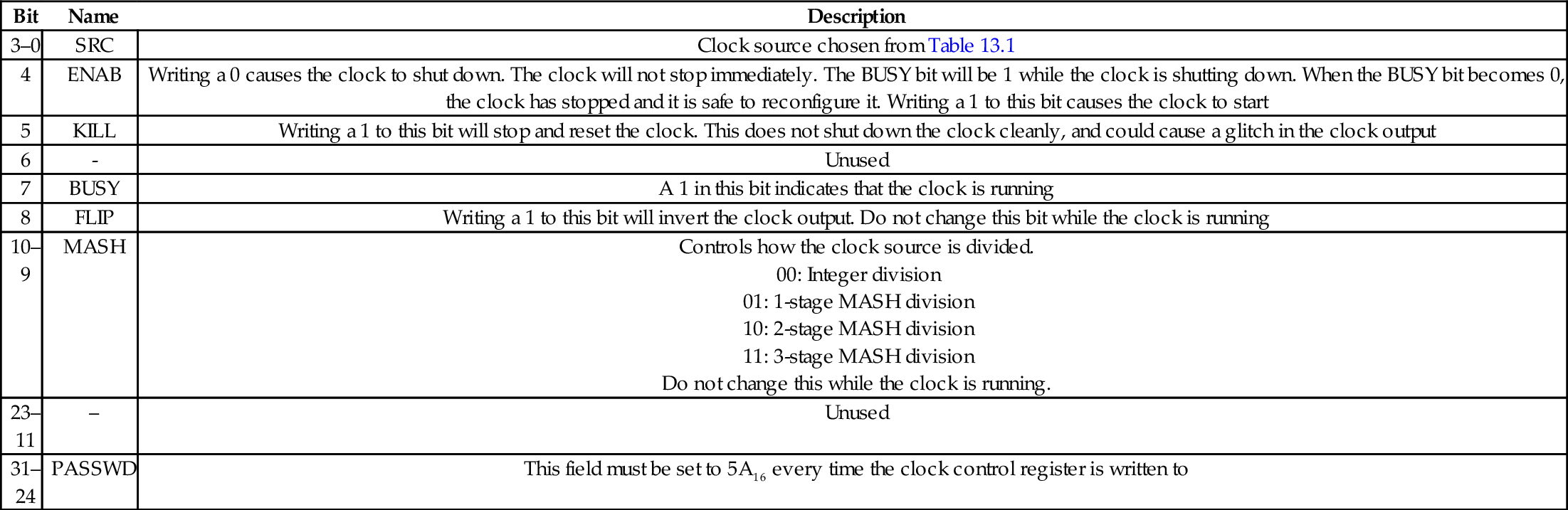
Table 13.4
Bit fields in the clock manager divisor registers
| Bit | Name | Description |
| 11–0 | DIVF | Fractional part of divisor. Do not change this while the clock is running |
| 23–12 | DIVI | Integer part of divisor. Do not change this while the clock is running |
| 31–24 | PASSWD | This field must be set to 5A16 every time the clock divisor register is written to |
1. Read the desired clock control register.
2. Clear bit 4 in the word that was read, then OR it with 5A00000016 and store the result back to the desired clock control register.
3. Repeatedly read the desired clock control register, until bit 7 becomes 0.
4. Calculate the divisor required and store it into the desired clock divisor register.
5. Create a word to configure and start the clock. Begin with 5A00000016, and set bits 3–0 to select the desired clock source. Set bits 10–9 to select the type of division, and set bit 4 to 1 to enable the clock.
6. Store the control word into the desired clock control register.
Selection of the divisor depends on which clock source is used, what type of division is selected, and the desired output of the clock being configured. For example, to set the PWM clock to 100 kHz, the 19.20 MHz clock can be used. Dividing that clock by 192 will provide a 100-KHz clock. To accomplish this, it is necessary to stop the PWM clock as described, store the value 5A0C000016 in the PWM clock divisor register, and then start the clock by writing 5A00001116 into the PWM clock control register.
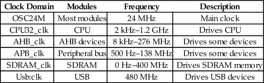
13.1.2 pcDuino Clock Control Unit
The AllWinner A10/A20 SOCs have a relatively simple clock manager, which is referred to as the Clock Control Unit. All of the clock signals in the system are driven by two crystal oscillators: the main oscillator runs at 24 MHz, and the real-time-clock oscillator, which runs at 32768 Hz. The real-time-clock oscillator is used only to provide a signal to the real-time-clock device.
The main clock oscillator drives many of the devices in the system, but there are seven phase-locked-loop circuits in the CCU which provide signals for devices which need clocks that are faster or slower than 24 MHz. Table 13.5 shows which devices are driven by the nine clock signals.
Table 13.5
Clock signals in the AllWinner A10/A20 SOC
| Clock Domain | Modules | Frequency | Description |
| OSC24M | Most modules | 24 MHz | Main clock |
| CPU32_clk | CPU | 2 kHz–1.2 GHz | Drives CPU |
| AHB_clk | AHB devices | 8 kHz–276 MHz | Drives some devices |
| APB_clk | Peripheral bus | 500 Hz–138 MHz | Drives some devices |
| SDRAM_clk | SDRAM | 0 Hz–400 MHz | Drives SDRAM memory |
| Usb:clk | USB | 480 MHz | Drives USB devices |
13.2 Serial Communications
There are basically two methods for transferring data between two digital devices: parallel and serial. Parallel connections use multiple wires to carry several bits at one time, typically including extra wires to carry timing information. Parallel communications are used for transferring large amounts of data over very short distances. However, this approach becomes very expensive when data must be transferred more than a few meters. Serial, on the other hand, uses a single wire to transfer the data bits one at a time. When compared to parallel transfer, the speed of serial transfer typically suffers. However, because it uses significantly fewer wires, the distance may be greatly extended, reliability improved, and cost vastly reduced.
13.2.1 UART
One of the oldest and most common devices for communications between computers and peripheral devices is the Universal Asynchronous Receiver/Transmitter, or UART. The word “universal” indicates that the device is highly configurable and flexible. UARTs allow a receiver and transmitter to communicate without a synchronizing signal.
The logic signal produced by the digital UART typically oscillates between zero volts for a low level and five volts for a high level, and the amount of current that the UART can supply is limited. For transmitting the data over long distances, the signals may go through a level-shifting or amplification stage. The circuit used to accomplish this is typically called a line driver. This circuit boosts the signal provided by the UART and also protects the delicate digital outputs from short circuits and signal spikes. Various standards, such as RS-232, RS-422, and RS-485 define the voltages that the line driver uses. For example, the RS-232 standard specifies that valid signals are in the range of + 3 to + 15 V, or − 3 to − 15 V. The standards also specify the maximum time that is allowable when shifting from a high signal to a low signal and vice versa, the amount of current that the device must be capable of sourcing and sinking, and other relevant design criteria.
The UART transmits data by sending each bit sequentially. The receiving UART re-assembles the bits into the original data. Fig. 13.2 shows how the transmitting UART converts a byte of data into a serial signal, and how the receiving UART samples the signal to recover the original data. Serializing the transmission and reassembly of the data are accomplished using shift registers. The receiver and transmitter each have their own clocks, and are configured so that the clocks run at the same speed (or close to the same speed). In this case, the receiver’s clock is running slightly slower than the transmitter’s clock, but the data are still received correctly.
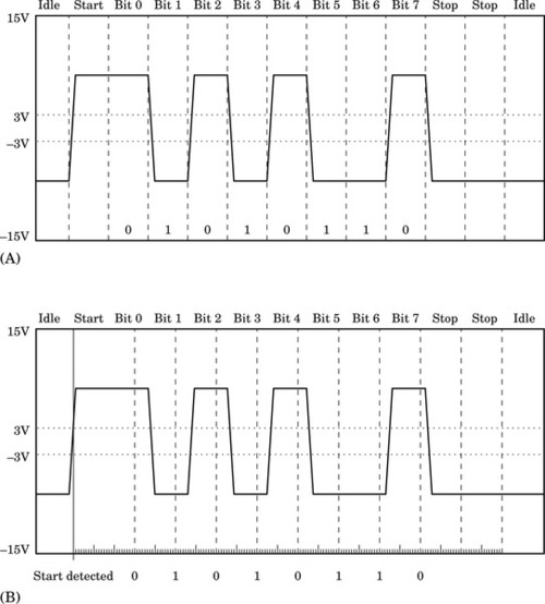
To transfer a group of bits, called a data frame, the transmitter typically first sends a start bit. Most UARTs can be configured to transfer between four and eight data bits in each group. The transmitting and receiving UARTS must be configured to use the same number of data bits. After each group of data bits, the transmitter will return the signal to the low state and keep it there for some minimum period. This period is usually the time that it would take to send two bits of data, and is referred to as the two stop bits. The stop bits allow the receiver to have some time to process the received byte and prepare for the next start bit. Fig. 13.2A shows what a typical RS-232 signal would look like when transferring the value 5616 (the ASCII “V” character). The UART enters the idle state only if there is not another byte immediately ready to send. If the transmitter has another byte to send, then the start bit can begin at the end of the second stop bit.
Note that it is impossible to ensure that the receiver and transmitter have clocks which are running at exactly the same speed, unless they use the same clock signal. Fig. 13.2B shows how the receiver can reassemble the original data, even with a slightly different clock rate. When the start bit is detected by the receiver, it prepares to receive the data bits, which will be sent by the transmitter at an expected rate (within some tolerance). The receive circuitry of most UARTS is driven by a clock that runs 16 times as fast as the baud rate. The receive circuitry uses its faster clock to latch each bit in the middle of its expected time period. In Fig. 13.2B, the receiver clock is running slower than the transmitter clock. By the end of the data frame, the sample time is very far from the center of the bit, but the correct value is received. If the clocks differed by much more, or if more than eight data bits were sent, then it is very likely that incorrect data would be received. Thus, as long as their clocks are synchronized within some tolerance (which is dependent on the number of data bits and the baud rate), the data will be received correctly.
The RS-232 standard allows point-to-point communication between two devices for limited distances. With the RS-232 standard, simple one-way communications can be accomplished using only two wires: One to carry the serial bits, and another to provide a common ground. For bi-directional communication, three wires are required. In addition, the RS-232 standard specifies optional hand-shaking signals, which the UARTs can use to signal their readiness to transmit or receive data. The RS-422 and RS-485 standards allow multiple devices to be connected using only two wires.
The first UART device to enjoy widespread use was the 8250. The original version had 12 registers for configuration, sending, and receiving data. The most important registers are the ones that allow the programmer to set the transmit and receive bit rates, or baud. One baud is one bit per second. The baud is set by storing a 16 bit divisor in two of the registers in the UART. The chip is driven by an external clock, and the divisor is used to reduce the frequency of the external clock to a frequency that is appropriate for serial communication. For example, if the external clock runs at 1 MHz, and the required baud is 1200, then the divisor must be  . Note that the divisor can only be an integer, so the device cannot achieve exactly 1200 baud. However, as explained previously, the sending and receiving devices do not have to agree precisely on the baud. During the transmission and reception of a byte, 1200.48 baud is close enough that the bits will be received correctly even if the other end is running slightly below 1200 baud. In the 8250, there was only one 8-bit register for sending data and only one 8-bit register for receiving data. The UART could send an interrupt to the CPU after each byte was transmitted or received. When receiving, the CPU had to respond to the interrupt very quickly. If the current byte was not read quickly enough by the CPU, it would be overwritten by the subsequent incoming byte. When transmitting, the CPU needed to respond quickly to interrupts to provide the next byte to be sent, or the transmission rate would suffer.
The next generation of UART device was the 16550A. This device is the model for most UART devices today. It features 16-byte input and output buffers and the ability to trigger interrupts when a buffer is partially full or partially empty. This allows the CPU to move several bytes of data at a time and results in much lower CPU overhead and much higher data transmission and reception rates. The 16550A also supports much higher baud rates than the 8250.
13.2.2 Raspberry Pi UART0
The BCM2835 system-on-chip provides two UART devices: UART0 and UART1. UART 1 is part of the I2C device, and is not recommended for use as a UART. UART0 is a PL011 UART, which is based on the industry standard 16550A UART. The major differences are that the PL011 allows greater flexibility in configuring the interrupt trigger levels, the registers appear in different locations, and the locations of bits in some of the registers is different. So, although it operates very much like a 16550A, things have been moved to different locations. The transmit and receive lines can be routed through GPIO pin 14 and GPIO pin 15, respectively. UART0 has 18 registers, starting at its base address of 2E2010016. Table 13.6 shows the name, location, and a brief description for each of the registers.
Table 13.6
Raspberry Pi UART0 register map
| Offset | Name | Description |
| 0016 | UART_DR | Data Register |
| 0416 | UART_RSRECR | Receive Status Register/Error Clear Register |
| 1816 | UART_ FR | Flag register |
| 2016 | UART_ILPR | not in use |
| 2416 | UART_IBRD | Integer Baud rate divisor |
| 2816 | UART_FBRD | Fractional Baud rate divisor |
| 2c16 | UART_LCRH | Line Control register |
| 3016 | UART_CR | Control register |
| 3416 | UART_IFLS | Interrupt FIFO Level Select Register |
| 3816 | UART_IMSC | Interrupt Mask Set Clear Register |
| 3c16 | UART_RIS | Raw Interrupt Status Register |
| 4016 | UART_MIS | Masked Interrupt Status Register |
| 4416 | UART_ICR | Interrupt Clear Register |
| 4816 | UART_DMACR | DMA Control Register |
| 8016 | UART_ITCR | Test Control register |
| 8416 | UART_ITIP | Integration test input reg |
| 8816 | UART_ITOP | Integration test output reg |
| 8c16 | UART_TDR | Test Data reg |
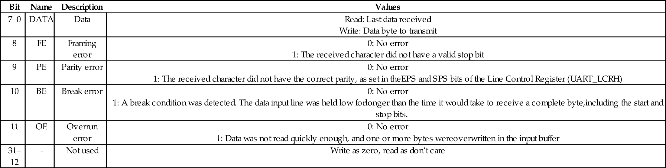
UART_DR: The UART Data Register is used to send and receive data. Data are sent or received one byte at a time. Writing to this register will add a byte to the transmit FIFO. Although the register is 32 bits, only the 8 least significant bits are used in transmission, and 12 least significant bits are used for reception. If the FIFO is empty, then the UART will begin transmitting the byte immediately. If the FIFO is full, then the last byte in the FIFO will be overwritten with the new byte that is written to the Data Register. When this register is read, it returns the byte at the top of the receive FIFO, along with four additional status bits to indicate if any errors were encountered. Table 13.7 specifies the names and use of the bits in the UART Data Register.
Table 13.7
Raspberry Pi UART data register
| Bit | Name | Description | Values |
| 7–0 | DATA | Data |
Write: Data byte to transmit |
| 8 | FE | Framing error |
1: The received character did not have a valid stop bit |
| 9 | PE | Parity error |
1: The received character did not have the correct parity, as set in theEPS and SPS bits of the Line Control Register (UART_LCRH) |
| 10 | BE | Break error |
1: A break condition was detected. The data input line was held low forlonger than the time it would take to receive a complete byte,including the start and stop bits. |
| 11 | OE | Overrun error |
1: Data was not read quickly enough, and one or more bytes wereoverwritten in the input buffer |
| 31–12 | - | Not used | Write as zero, read as don’t care |
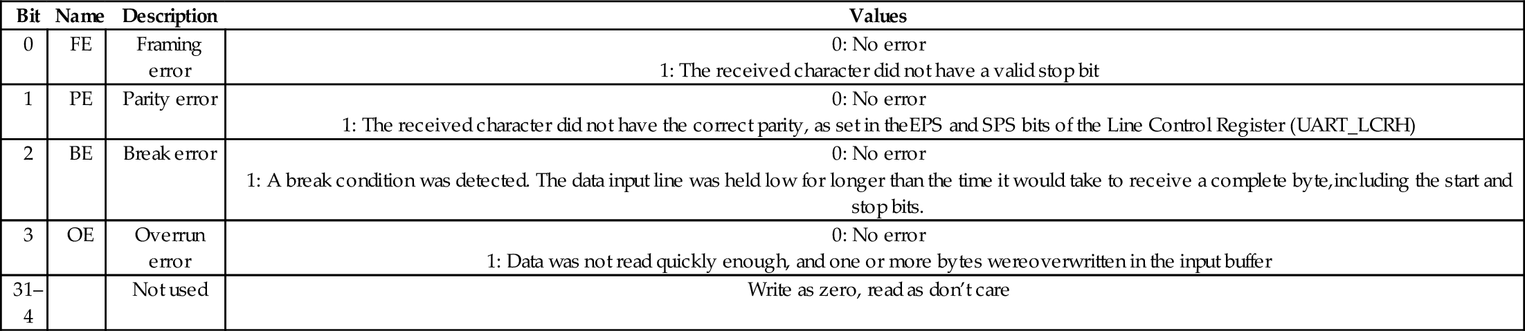
UART_RSRECR: The UART Receive Status Register/Error Clear Register is used to check the status of the byte most recently read from the UART Data Register, and to check for overrun conditions at any time. The status information for overrun is set immediately when an overrun condition occurs. The Receive Status Register/Error Clear Register provides the same four status bits as the Data Register (but in bits 3–0 rather than bits 11–8). The received data character must be read first from the Data Register, before reading the error status associated with that data character from the RSRECR register. Since the Data Register also contains these 4 bits, this register may not be required, depending on how the software is written. Table 13.8 describes the bits in this register.
Table 13.8
Raspberry Pi UART receive status register/error clear register
| Bit | Name | Description | Values |
| 0 | FE | Framing error |
1: The received character did not have a valid stop bit |
| 1 | PE | Parity error |
1: The received character did not have the correct parity, as set in theEPS and SPS bits of the Line Control Register (UART_LCRH) |
| 2 | BE | Break error |
1: A break condition was detected. The data input line was held low for longer than the time it would take to receive a complete byte,including the start and stop bits. |
| 3 | OE | Overrun error |
1: Data was not read quickly enough, and one or more bytes wereoverwritten in the input buffer |
| 31–4 | Not used | Write as zero, read as don’t care |
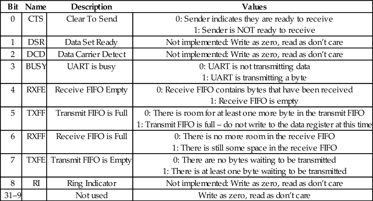
UART_FR: The UART Flag Register can be read to determine the status of the UART. The bits in this register are used mainly when sending and receiving data using the FIFOs. When several bytes need to be sent, the TXFF flag should be checked to ensure that the transmit FIFO is not full before each byte is written to the data register. When receiving data, the RXFE bit can be used to determine whether or not there is more data to be read from the FIFO. Table 13.9 describes the flags in this register.
Table 13.9
Raspberry Pi UART flags register bits
UART_ILPR: This is the IrDA register, which is supported by some PL011 UARTs. IrDA stands for the Infrared Data Association, which is a group of companies that cooperate to provide specifications for a complete set of protocols for wireless infrared communications. The name “IrDA” also refers to that set of protocols. IrDA is not implemented on the Raspberry Pi UART. Writing to this register has no effect and reading returns 0.
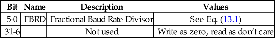
UART_IBRD and UART_FBRD: UART_FBRD is the fractional part of the baud rate divisor value, and UART_IBRD is the integer part. The baud rate divisor is calculated as follows:

where UARTCLK is the frequency of the UART_CLK that is configured in the Clock Manager device. The default value is 3 MHz. BAUDDIV is stored in two registers. UART_IBRD holds the integer part and UART_FBRD holds the fractional part. Thus BAUDDIV should be calculated as a U(16,6) fixed point number. The contents of the UART_IBRD and UART_FBRD registers may be written at any time, but the change will not have any effect until transmission or reception of the current character is complete. Table 13.10 shows the arrangement of the integer baud rate divisor register, and Table 13.11 shows the arrangement of the fractional baud rate divisor register.
Table 13.10
Raspberry Pi UART integer baud rate divisor
| Bit | Name | Description | Values |
| 15–0 | IBRD | Integer Baud Rate Divisor | See Eq. (13.1) |
| 31–16 | Not used | Write as zero, read as don’t care |
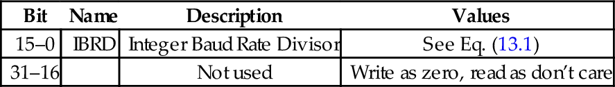
Table 13.11
Raspberry Pi UART fractional baud rate divisor
| Bit | Name | Description | Values |
| 5-0 | FBRD | Fractional Baud Rate Divisor | See Eq. (13.1) |
| 31-6 | Not used | Write as zero, read as don’t care |
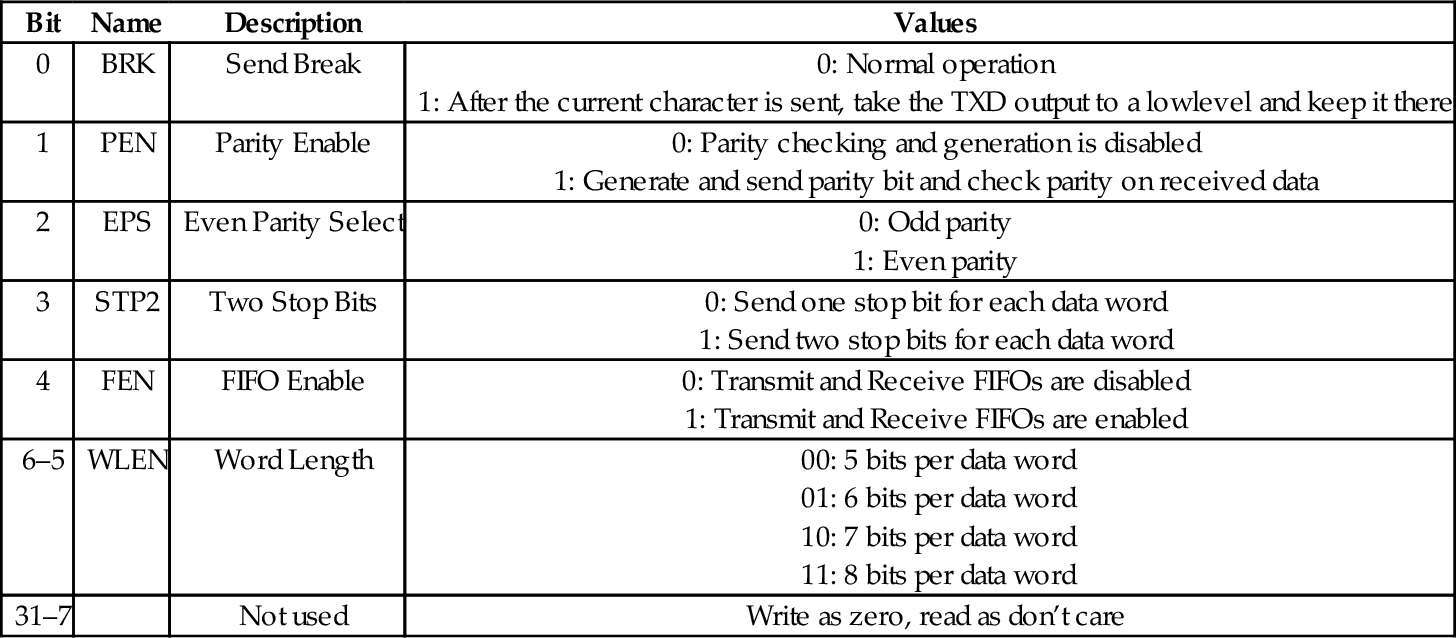
UART_LCRH: UART_LCRH is the line control register. It is used to configure the communication parameters. This register must not be changed until the UART is disabled by writing zero to bit 0 of UART_CR, and the BUSY flag in UART_FR is clear. Table 13.12 shows the layout of the line control register.
Table 13.12
Raspberry Pi UART line control register bits
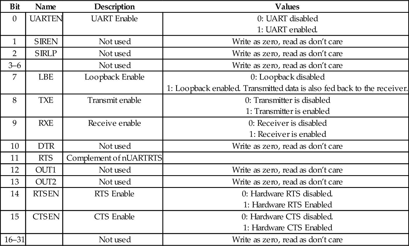
UART_CR: The UART Control Register is used for configuring, enabling, and disabling the UART. Table 13.13 shows the layout of the control register. To enable transmission, the TXE bit and UARTEN bit must be set to 1. To enable reception, the RXE bit and UARTEN bit must be set to 1. In general, the following steps should be used to configure or re-configure the UART:
Table 13.13
Raspberry Pi UART control register bits
| Bit | Name | Description | Values |
| 0 | UARTEN | UART Enable |
1: UART enabled. |
| 1 | SIREN | Not used | Write as zero, read as don’t care |
| 2 | SIRLP | Not used | Write as zero, read as don’t care |
| 3–6 | Not used | Write as zero, read as don’t care | |
| 7 | LBE | Loopback Enable |
1: Loopback enabled. Transmitted data is also fed back to the receiver. |
| 8 | TXE | Transmit enable |
1: Transmitter is enabled |
| 9 | RXE | Receive enable |
1: Receiver is enabled |
| 10 | DTR | Not used | Write as zero, read as don’t care |
| 11 | RTS | Complement of nUARTRTS | |
| 12 | OUT1 | Not used | Write as zero, read as don’t care |
| 13 | OUT2 | Not used | Write as zero, read as don’t care |
| 14 | RTSEN | RTS Enable |
1: Hardware RTS Enabled |
| 15 | CTSEN | CTS Enable |
1: Hardware CTS Enabled |
| 16–31 | Not used | Write as zero, read as don’t care |
(b) Wait for the end of transmission or reception of the current character.
(c) Flush the transmit FIFO by setting the FEN bit to 0 in the Line Control Register.
(d) Reprogram the Control Register.
(e) Enable the UART.
Interrupt Control: The UART can signal the CPU by asserting an interrupt when certain conditions occur. This will be covered in more detail in Chapter 14. For now, it is enough to know that there are five additional registers which are used to configure and use the interrupt mechanism.
UART_IFLS defines the FIFO level that triggers the assertion of the interrupt signal. One interrupt is generated when the FIFO reaches the specified level. The CPU must clear the interrupt before another can be generated.
UART_IMSC is the interrupt mask set/clear register. It is used to enable or disable specific interrupts. This register determines which of the possible interrupt conditions are allowed to generate an interrupt to the CPU.
UART_RIS is the raw interrupt status register. It can be read to raw status of interrupts conditions before any masking is performed.
UART_MIS is the masked interrupt status register. It contains the masked status of the interrupts. This is the register that the operating system should use to determine the cause of a UART interrupt.
UART_ICR is the interrupt clear register. writing to it clears the interrupt conditions. The operating system should use this register to clear interrupts before returning from the interrupt service routine.
UART_DMACR: The DMA control register is used to configure the UART to access memory directly, so that the CPU does not have to move each byte of data to or from the UART. DMA will be explained in more detail in Chapter 14.
Additional Registers: The remaining registers, UART_ITCR, UART_ITIP, and UART_ITOP, are either unimplemented or are used for testing the UART. These registers should not be used.
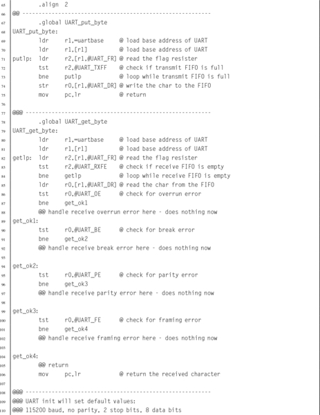
13.2.3 Basic Programming for the Raspberry Pi UART
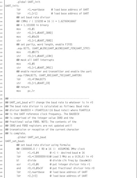
Listing 13.1 shows four basic functions for initializing the UART, changing the baud rate, sending a character, and receiving a character using UART0 on the Raspberry Pi. Note that a large part of the code simply defines the location and offset for all of the registers (and bits) that can be used to control the UART.

13.2.4 pcDuino UART
The AllWinner A10/A20 SOC includes eight UART devices. They are all fully compatible with the 16550A UART, and also provide some enhancements. All of them provide transmit (TX) and receive (RX) signals. UART0 has the full set of RS232 signals, including RTS, CTS, DTR, DSR, DCD, and RING. UART1 has the RTS and CTS signals. The remaining six UARTs only provide the TX and RX signals. They can all be configured for serial IrDA. Table 13.14 shows the base address for each of the eight UART devices.
Table 13.14
pcDuino UART addresses
| Name | Address |
| UART0 | 0x01C28000 |
| UART1 | 0x01C28400 |
| UART2 | 0x01C28800 |
| UART3 | 0x01C28C00 |
| UART4 | 0x01C29000 |
| UART5 | 0x01C29400 |
| UART6 | 0x01C29800 |
| UART7 | 0x01C29C00 |
When the 16550 UART was designed, 8-bit processors were common, and most of them provided only 16 address bits. Memory was typically limited to 64 kB, and every byte of address space was important. Because of these considerations, the designers of the 16550 decided to limit the number of addresses used to 8, and to only use eight bits of data per address. There are 10 registers in the 16550 UART, but some of them share the same address. For example, there are three registers mapped to an offset address of zero, two registers mapped at offset four, and two registers mapped at offset eight. Bit seven in the Line Control Register is used to determine which of the registers is active for a given address.
Because they are meant to be fully backwards-compatible with the 16550, the AllWinner A10/A20 SOC UART devices also use only 8 bits for each register, and the first 12 registers correspond exactly with the 16550 UART. The only differences are that the pcDuino uses word addresses rather than byte addresses, and they provide four additional registers that are used for IrDA mode. Table 13.15 shows the arrangement of the registers in each of the 8 UARTs on the pcDuino. The following sections will explain the registers.
Table 13.15
pcDuino UART register offsets
| Register Name | Offset | Description |
| UART_RBR | 0x00 | UART Receive Buffer Register |
| UART_THR | 0x00 | UART Transmit Holding Register |
| UART_DLL | 0x00 | UART Divisor Latch Low Register |
| UART_DLH | 0x04 | UART Divisor Latch High Register |
| UART_IER | 0x04 | UART Interrupt Enable Register |
| UART_IIR | 0x08 | UART Interrupt Identity Register |
| UART_FCR | 0x08 | UART FIFO Control Register |
| UART_LCR | 0x0C | UART Line Control Register |
| UART_MCR | 0x10 | UART Modem Control Register |
| UART_LSR | 0x14 | UART Line Status Register |
| UART_MSR | 0x18 | UART Modem Status Register |
| UART_SCH | 0x1C | UART Scratch Register |
| UART_USR | 0x7C | UART Status Register |
| UART_TFL | 0x80 | UART Transmit FIFO Level |
| UART_RFL | 0x84 | UART_RFL |
| UART_HALT | 0xA4 | UART Halt TX Register |
The baud rate is set using a 16-bit Baud Rate Divisor, according to the following equation:

where sclk is the frequency of the UART serial clock, which is configured by the Clock Manager device. The default frequency of the clock is 24 MHz. BAUDDIV is stored in two registers. UART_DLL holds the least significant 8 bits, and UART_DLH holds the most significant 8 bits. Thus BAUDDIV should be calculated as a 16-bit unsigned integer. Note that for high baud rates, it may not be possible to get exactly the rate desired. For example, a baud rate of 115200 would require a divisor of  . Since the baud rate divisor can only be given as an integer, the desired rate must be based on a divisor of 13, so the true baud rate will be
  , or about 0.16% faster than desired. Although slightly fast, it is well within the tolerance for RS232 communication.
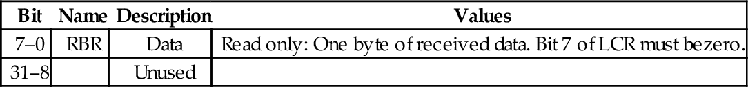
UART_RBR: The UART Receive Buffer Register is used to receive data, 1 byte at a time. If the receive FIFO is enabled, then as the UART receives data, it places the data into a receive FIFO. Reading from this address removes 1 byte from the receive FIFO. If the FIFO becomes full and another data byte arrives, then the new data are lost and an overrun error occurs. Table 13.16 shows the layout of the receive buffer register.
Table 13.16
pcDuno UART receive buffer register
| Bit | Name | Description | Values |
| 7–0 | RBR | Data | Read only: One byte of received data. Bit 7 of LCR must bezero. |
| 31–8 | Unused |
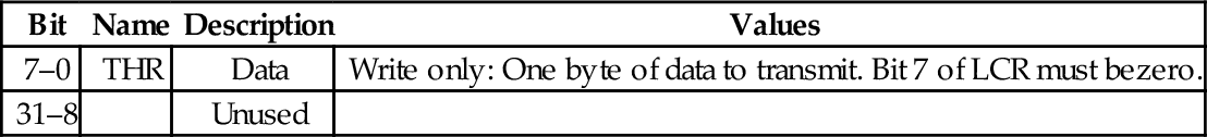
UART_THR: Writing to the Transmit Holding Register will cause that byte to be transmitted by the UART. If the transmit FIFO is enabled, then the byte will be added to the end of the transmit FIFO. If the FIFO is empty, then the UART will begin transmitting the byte immediately. If the FIFO is full, then the new data byte will be lost. Table 13.17 shows the layout of the transmit holding register.
Table 13.17
pcDuno UART transmit holding register
| Bit | Name | Description | Values |
| 7–0 | THR | Data | Write only: One byte of data to transmit. Bit 7 of LCR must bezero. |
| 31–8 | Unused |
UART_DLL: The UART Divisor Latch Low register is used to set the least significant byte of the baud rate divisor. When bit 7 of the Line Control Register is set to one, writing to this address will access the DLL register. If bit 7 of the Line Control Register is set to zero, then writing to this address will access the transmit holding register. Table 13.18 shows the layout of the UART_DLL register.
Table 13.18
pcDuno UART divisor latch low register
| Bit | Name | Description | Values |
| 7–0 | DLL | Data | Write only: Least significant eight bits of the Baud Rate Divisor. Bit 7 of LCR must be one. |
| 31–8 | Unused |

UART_DLH: The UART Divisor Latch High register is used to set the most significant byte of the baud rate divisor. When bit 7 of the Line Control Register is set to one, writing to this address will access the DLH register. If bit 7 of the Line Control Register is set to zero, then writing to this address will access the Interrupt Enable Register rather than the Divisor Latch High register. Table 13.19 shows the layout of the UART_DLL register.
If the two Divisor Latch Registers (DLL and DLH) are set to zero, the baud clock is disabled and no serial communications occur. DLH should be set before DLL, and at least eight clock cycles of the UART clock should be allowed to pass before data are transmitted or received.
Table 13.19
pcDuno UART divisor latch high register
| Bit | Name | Description | Values |
| 7–0 | DLH | Data | Write only: Most significant eight bits of the Baud Rate Divisor. Bit 7 of LCR must be one. |
| 31–8 | Unused |

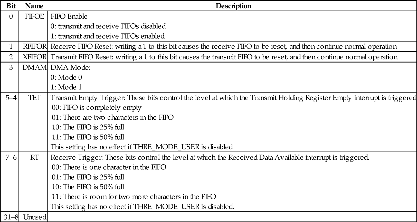
UART_FCR: is the UART FIFO control register. It is used to enable or disable the receive and transmit FIFOs (buffers), flush their contents, set the level at which the transmit and receive FIFOs trigger an interrupt, and to control Direct Memory Access (DMA) Table 13.20 shows the layout of the UART_FCR register.
Table 13.20
pcDuno UART FIFO control register
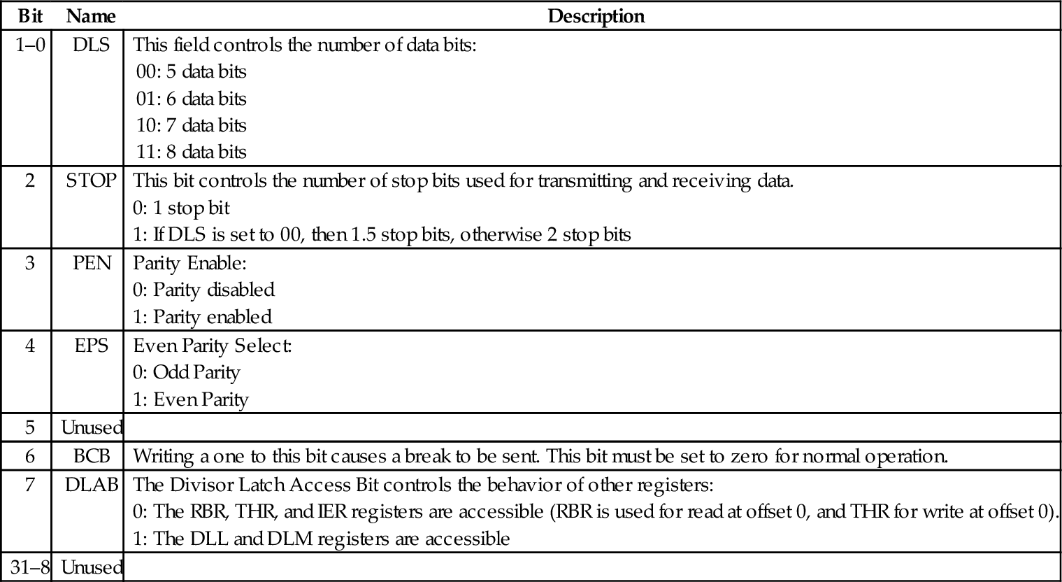
UART_LCR: The Line Control Register is used to control the parity, number of data bits, and number of stop bits for the serial port. Bit 7 also controls which registers are mapped at offsets 0, 4, and 8 from the device base address. Table 13.21 shows the layout of the UART_LCR register.
Table 13.21
pcDuno UART line control register
UART_LSR: The Line Status Register is used to read status information from the UART. Table 13.22 shows the layout of the UART_LSR register.
Table 13.22
pcDuno UART line status register
| Bit | Name | Description |
| 0 | DR | When the Data Ready bit is set to 1, it indicates that at least one byte is ready to be read from the receive FIFO or RBR. |
| 1 | OE | When the Overrun Error bit is set to 1, it indicates that an overrun error occurred for the byte at the top of the receive FIFO. |
| 2 | PE | When the Parity Error bit is set to 1, it indicates that a parity error occurred for the byte at the top of the receive FIFO. |
| 3 | FE | When the Framing Error bit is set to 1, it indicates that a framing error occurred for the byte at the top of the receive FIFO. |
| 4 | BI | When the Break Interrupt bit is set to 1, it indicates thata break has been received. |
| 5 | THRE | When the Transmit Holding Register Empty bit is 1, it indicates that there are there are no bytes waiting to be transmitted, but there may be a byte currently being transmitted. |
| 6 | TEMT | When the Transmitter Empty bit is 1, it indicates that there are no bytes waiting to be transmitted and no byte currently being transmitted. |
| 7 | FIFOERR | When this bit is 1, an error has occurred (PE, BE, or BI) in the receive FIFO. This bit is cleared when the Line Status Register is read. |
| 31–8 | Unused |
UART_USR: The UART Status Register is used to read information about the status of the transmit and receive FIFOs, and the current state of the receiver and transmitter. Table 13.23 shows the layout of the UART_USR register. This register contains essentially the same information as the status register in the Raspberry Pi UART.
Table 13.23
pcDuno UART status register
| Bit | Name | Description |
| 0 | BUSY | When the Busy bit is 1, it indicates that the UART is currently busy. When it is 0, the UART is idle or inactive. |
| 1 | TFNF | When the Transmit FIFO Not Full bit is 1, it indicates that at least one more byte can be safely written to the Transmit FIFO. |
| 2 | TFE | When the Transmit FIFO Empty bit is 1, it indicates that there are no bytes remaining in the transmit FIFO. |
| 3 | RFNE | When the Receive FIFO Not Empty bit is 1, it indicates that at least one more byte is waiting to be read from the receive FIFO. |
| 4 | RFF | When the Receive FIFO Full bit is 1, it indicates that there is no more room in the receive FIFO. If data is not read before the next character is received, an overrun error will occur. |
| 31–5 | Unused |
UART_TFL: The UART Transmit FIFO Level register allows the programmer to determine exactly how many bytes are currently in the transmit FIFO. Table 13.24 shows the layout of the UART_TFL register.
Table 13.24
pcDuno UART transmit FIFO level register
| Bit | Name | Description |
| 6–0 | TFL | The Transmit FIFO level field contains an integer which indicates the number of bytes currently in the transmit FIFO. |
| 31–7 | Unused |
UART_RFL: The UART Receive FIFO Level register allows the programmer to determine exactly how many bytes are currently in the receive FIFO. Table 13.25 shows the layout of the UART_RFL register.
Table 13.25
pcDuno UART receive FIFO level register
| Bit | Name | Description |
| 6–0 | RFL | The Receive FIFO level field contains an integer which indicates the number of bytes currently in the receive FIFO. |
| 31–7 | Unused |
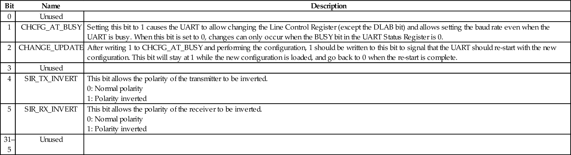
UART_HALT: The UART transmit halt register is used to halt the UART so that it can be reconfigured. After the configuration is performed, it is then used to signal the UART to restart with the new settings. It can also be used to invert the receive and transmit polarity. Table 13.26 shows the layout of the UART_HALT register.
Table 13.26
pcDuno UART transmit halt register
| Bit | Name | Description |
| 0 | Unused | |
| 1 | CHCFG_AT_BUSY | Setting this bit to 1 causes the UART to allow changing the Line Control Register (except the DLAB bit) and allows setting the baud rate even when the UART is busy. When this bit is set to 0, changes can only occur when the BUSY bit in the UART Status Register is 0. |
| 2 | CHANGE_UPDATE | After writing 1 to CHCFG_AT_BUSY and performing the configuration, 1 should be written to this bit to signal that the UART should re-start with the new configuration. This bit will stay at 1 while the new configuration is loaded, and go back to 0 when the re-start is complete. |
| 3 | Unused | |
| 4 | SIR_TX_INVERT | This bit allows the polarity of the transmitter to be inverted.
1: Polarity inverted |
| 5 | SIR_RX_INVERT | This bit allows the polarity of the receiver to be inverted.
1: Polarity inverted |
| 31–5 | Unused |
Interrupt Control: The UART can signal the CPU by asserting an interrupt when certain conditions occur. This will be covered in more detail in Chapter 14. For now, it is enough to know that there are five additional registers which are used to configure and use the interrupt mechanism.
UART_IFLS defines the FIFO level that triggers the assertion of the interrupt signal. One interrupt is generated when the FIFO reaches the specified level. The CPU must clear the interrupt before another can be generated.
UART_IER is the interrupt enable register. It is used to enable or disable the generation of interrupts for specific conditions.
UART_IIR is the Interrupt Identity Register. When an interrupt occurs, the CPU can read this register to determine what caused the interrupt.
Additional Registers There are several additional registers which are not needed for basic use of the UART.
UART_MCR is the Modem Control Register. It is used to configure the port for IrDA mode, enable Automatic Flow Control, and manage the RS-232 RTS and DTR hardware handshaking signals for the ports in which they are implemented. The default configuration disables these extra features.
UART_MSR is the Modem Status Register, which is used to read the state of the RS-232 modem control and status lines on ports that implement them. This register can be ignored unless a telephone modem is being used on the port.
UART_SCH is the Modem Scratch Register. It provides 8 bits of storage for temporary data values. In the days of 8 and 16-bit computers, when the 16550 UART was designed, this extra byte of storage was useful.
13.3 Chapter Summary
Most modern computer systems have some type of Universal Asynchronous Receiver/Transmitter. These are serial communications devices, and are meant to provide communications with other systems using RS-232 (most commonly) or some other standard serial protocol. Modern systems often have a large number of other devices as well. Each device may need its own clock source to drive it at the correct frequency for its operation. The clock sources for all of the devices are often controlled by yet another device: the clock manager.
Although two systems may have different UARTs, these devices perform the same basic functions. The specifics about how they are programmed will vary from one system to another. However, there is always enough similarity between devices of the same class that a programmer who is familiar with one specific device can easily learn to program another similar device. The more experience a programmer has, the less time it takes to learn how to control a new device.
Exercises
13.1 Write a function for setting the PWM clock on the Raspberry Pi to 2 MHz.
13.2 The UART_GET_BYTE function in Listing 13.1 contains skeleton code for handling errors, but does not actually do anything when errors occur. Describe at least two ways that the errors could be handled.
13.3 Listing 13.1 provides four functions for managing the UART on the Raspberry Pi. Write equivalent functions for the pcDuino UART.