Table of Contents for
Modern Assembly Language Programming with the ARM Processor
 Modern Assembly Language Programming with the ARM Processor
Published by
Newnes, 2016
Modern Assembly Language Programming with the ARM Processor
Published by
Newnes, 2016
- Modern Assembly Language Programming with the ARM Processor
- Cover image
- Title page
- Table of Contents
- Copyright
- List of Tables
- List of Figures
- List of Listings
- Preface
- Companion Website
- Acknowledgments
- Part I: Assembly as a Language
- Chapter 1: Introduction
- Chapter 2: GNU Assembly Syntax
- Chapter 3: Load/Store and Branch Instructions
- Chapter 4: Data Processing and Other Instructions
- Chapter 5: Structured Programming
- Chapter 6: Abstract Data Types
- Part II: Performance Mathematics
- Chapter 7: Integer Mathematics
- Chapter 8: Non-Integral Mathematics
- Chapter 9: The ARM Vector Floating Point Coprocessor
- Chapter 10: The ARM NEON Extensions
- 10.10 Multiplication and Division
- Part III: Accessing Devices
- Chapter 11: Devices
- Chapter 12: Pulse Modulation
- Chapter 13: Common System Devices
- Chapter 14: Running Without an Operating System
- Index
Devices
Abstract
This chapter starts with a high-level explanation of how devices may be accessed in a modern computer system, and then explains that most devices on modern architectures are memory-mapped. Next, it explains how memory mapped devices can be accessed by user processes under Linux, by making use of the mmap system call. Code examples are given, showing how several devices can be mapped into the memory of a user-level program on the Raspberry Pi and pcDuino. Next the General Purpose I/O devices on both systems are explained, providing the reader with the opportunity to do a comparison between two different devices which perform almost precisely the same functions.
Keywords
Device; Memory map; General purpose I/O (GPIO); I/O Pin; Header; Pull-up and pull-down resistor; LED; Switch
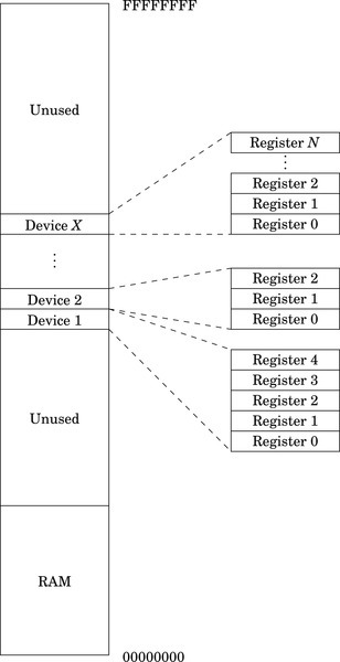
As mentioned in Chapter 1, a computer system consists of three main parts: the CPU, memory, and devices. The typical computing system has many devices of various types for performing specific functions. Some devices, such as data caches, are closely coupled to the CPU, and are typically controlled by executing special CPU instructions that can only be accessed in assembly language. However, most of the devices on a typical system are accessed and controlled through the system data bus. These devices appear to the programmer to be ordinary memory locations. The hardware in the system bus decodes the addresses coming from the CPU, and some addresses correspond to devices rather than memory. Fig. 11.1 shows the memory layout for a typical system. The exact locations of the devices and memory are chosen by the system hardware designers. From the programmer’s standpoint, writing data to certain memory addresses results in the data being transferred to a device rather than stored in memory. The programmer must read documentation on the hardware design to determine exactly where the devices are in memory.
11.1 Accessing Devices Directly Under Linux
There are devices that allow data to be read or written from external sources, devices that can measure time, devices for moving data from one location in memory to another, devices for modifying the addresses of memory regions, and devices for even more esoteric purposes. Some devices are capable of sending signals to the CPU to indicate that they need attention, while others simply wait for the CPU to check on their status.
A modern computer system, such as the Raspberry Pi, has dozens or even hundreds of devices. Programmers write device driver software for each device. A device driver provides a few standard function calls for each device, so that it can be used easily. The specific set of functions depends on the type of device and the design of the operating system. Operating system designers strive to define a small set of device types, and to define a standard software interface for each type in order to make devices interchangeable.
Devices are typically controlled by writing specific values to the device’s internal device registers. For the ARM processor, access to most device registers is accomplished using the load and store instructions. Each device is assigned a base address in memory. This address corresponds with the first register inside the device. The device may also have other registers that are accessible at some pre-defined offset address from the base address. Some registers are read-only, some are write-only, and some are read-write. To use the device, the programmer must read from, and write appropriate data to, the correct device registers. For every device, there is a programmer’s model and documentation explaining what each register in the device does. Some devices are well designed, easy to use, and well documented. Some devices are not, and the programmer must work harder to write software to use them.
Linux is a powerful, multiuser, multitasking operating system. The Linux kernel manages all of the devices and protects them from direct access by user programs. User programs are intended to access devices by making system calls. The kernel accesses the devices on behalf of the user programs, ensuring that an errant user program cannot misuse the devices and other resources on the system. Attempting to directly access the registers in any device will result in an exception. The kernel will take over and kill the offending process.
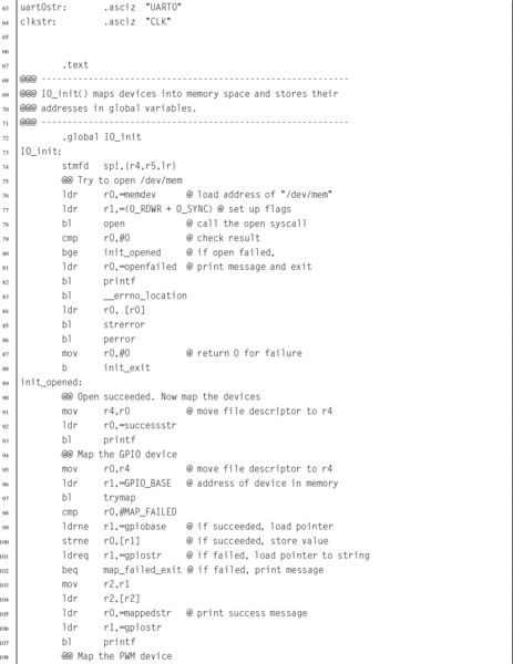
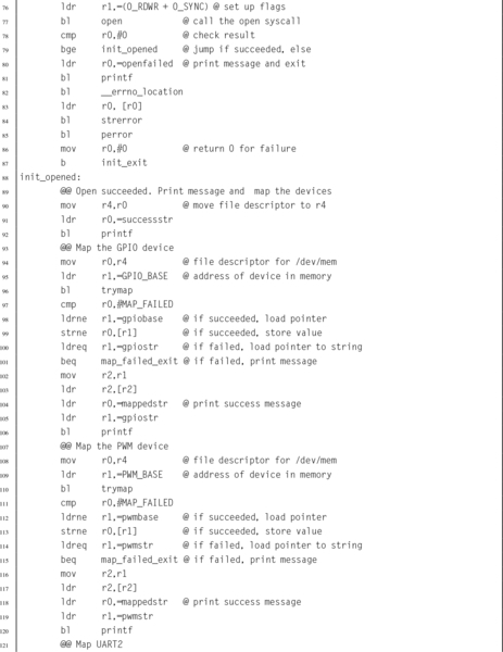
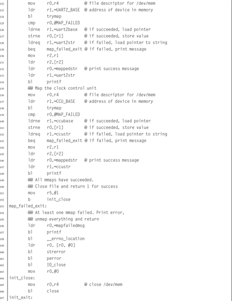
However, our programs will need direct access to the device registers. Linux allows user programs to gain direct access through the mmap() system call. Listing 11.1 shows how four devices can be mapped into the memory space of a user program on a Raspberry Pi. In most cases, the user program will need administrator privileges in order to perform the mapping. The operating system does not usually give permission for ordinary users to access devices directly. However Linux does provide the ability to change permissions on /dev/mem, or for user programs to run with elevated privileges.
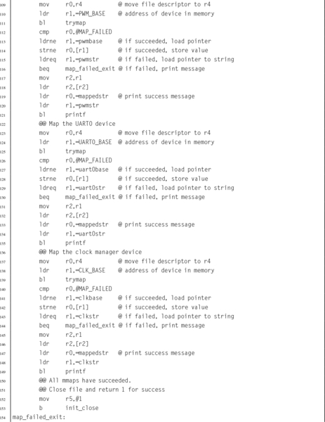
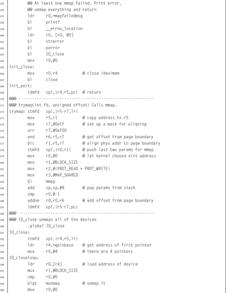

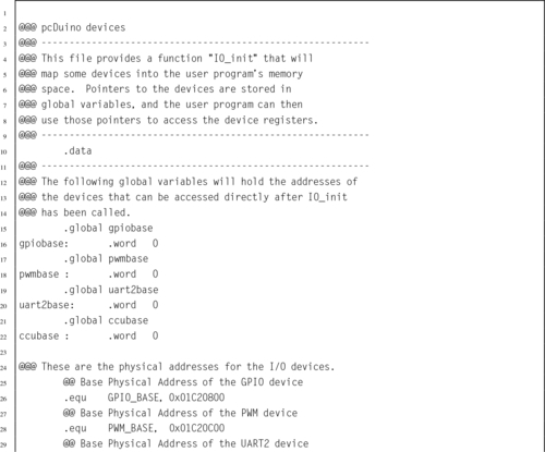
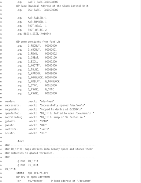
Listing 11.2 shows how four devices can be mapped into the memory space of a user program on a pcDuino. The devices are equivalent to the devices mapped in Listing 11.1. Some of the devices are described in the following sections of this chapter. The pcDuino devices and Raspberry Pi devices operate differently, but provide similar functionality. Note that most of the code is the same for both listings. The only real differences between Listings 11.1 and 11.2 are the names of the devices and their hardware addresses.
11.2 General Purpose Digital Input/Output
One type of device, commonly found on embedded systems, is the General Purpose I/O (GPIO) device. Although there are many variations on this device provided by different manufacturers, they all provide similar capabilities. The device provides a set of input and/or output bits, which allow signals to be transferred to or from the outside world. Each bit of input or output in a GPIO device is generally referred to as a pin, and a group of pins is referred to as a GPIO port. Ports commonly support 8 bits of input or output, but some devices have 16 or 32 bit ports. Some GPIO devices support multiple ports, and some systems have multiple GPIO devices in them.
A system with a GPIO device usually has some type of connector or wires that allow external inputs or outputs to be connected to the system. For example, the IBM PC has a type of GPIO device that was originally intended for communications with a parallel printer. On that platform, the GPIO device is commonly referred to as the parallel printer port.
Some GPIO devices, such as the one on the IBM PC, are arranged as sets of pins that can be switched as a group to either input or output. In many modern GPIO devices, each pin can be individually configured to accept or source different input and output voltages. On some devices, the amount of drive current available can be configured. Some include the ability to configure built-in pull-up and/or pull-down resistors. On most older GPIO devices, the input and output voltages are typically limited to the supply voltage of the GPIO device, and the device may be damaged by greater voltages. Newer GPIO devices generally can tolerate 5 V on inputs, regardless of the supply voltage of the device.
GPIO devices are very common in systems that are intended to be used for embedded applications. For most GPIO devices:
• individual pins or groups of pins can be configured,
• pins can be configured to be input or output,
• pins can be disabled so that they are neither input nor output,
• input values can be read by the CPU (typically high=1, low=0),
• output values can be read or written by the CPU, and
• input pins can be configured to generate interrupt requests.
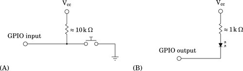
Some GPIO devices may also have more advanced features, such as the ability to use Direct Memory Access (DMA) to send data without requiring the CPU to move each byte or word. Fig. 11.2 shows two common ways to use GPIO pins. Fig. 11.2A shows a GPIO pin that has been configured for input, and connected to a push-button switch. When the switch is open, the pull-up resistor pulls the voltage on the pin to a high state. When the switch is closed, the pin is pulled to a low state and some current flows through the pull-up resistor to ground. Typically, the pull-up resistor would be around 10 kΩ. The specific value is not critical, but it must be high enough to limit the current to a small amount when the switch is closed. Fig. 11.2B shows a GPIO pin that is configured as an output and is being used to drive an LED. When a 1 is output on the pin, it is at the same voltage as Vcc (the power supply voltage), and no current flows. The LED is off. When a 0 is output on the pin, current is drawn through the resistor and the LED, and through the pin to ground. This causes the LED to be illuminated. Selection of the resistor is not critical, but it must be small enough to light the LED without allowing enough current to destroy either the LED or the GPIO circuitry. This is typically around 1 kΩ. Note that, in general, GPIO pins can sink more current than they can source, so it is most common to connect LEDs and other devices in the way shown.
11.2.1 Raspberry Pi GPIO
The Broadcom BCM2835 system-on-chip contains 54 GPIO pins that are split into two banks. The GPIO pins are named using the following format: GPIOx, where x is a number between 0 and 53. The GPIO pins are highly configurable. Each pin can be used for general purpose I/O, or can be configured to serve up to six pre-defined alternate functions. Configuring a GPIO pin for an alternate function usually allows some other device within the BCM2835 to use the pin. For example, GPIO4 can be used
• to send the signal generated by General Purpose Clock 0 to external devices,
• to send bit one of the Secondary Address Bus to external devices, or
• to receive JTAG data for programming the firmware of the device.
The last eight GPIO pins, GPIO46–GPIO53 have no alternate functions, and are used only for GPIO.
In addition to the alternate function, all GPIO pins can be configured individually as input or output. When configured as input, a pin can also be configured to detect when the signal changes, and to send an interrupt to the ARM CPU. Each input pin also has internal pull-up and pull-down resistors, which can be enabled or disabled by the programmer.
The GPIO pins on the BCM2835 SOC are very flexible and are quite complex, but are well designed and not difficult to program, once the programmer understands how the pins operate and what the various registers do. There are 41 registers that control the GPIO pins. The base address for the GPIO device is 20200000. The 41 registers and their offsets from the base address are shown in Table 11.1.
Table 11.1
Raspberry Pi GPIO register map
| Offset | Name | Description | Size | R/W |
| 0016 | GPFSEL0 | GPIO Function Select 0 | 32 | R/W |
| 0416 | GPFSEL1 | GPIO Function Select 1 | 32 | R/W |
| 0816 | GPFSEL2 | GPIO Function Select 2 | 32 | R/W |
| 0C16 | GPFSEL3 | GPIO Function Select 3 | 32 | R/W |
| 1016 | GPFSEL4 | GPIO Function Select 4 | 32 | R/W |
| 1416 | GPFSEL5 | GPIO Function Select 5 | 32 | R/W |
| 1C16 | GPSET0 | GPIO Pin Output Set 0 | 32 | W |
| 2016 | GPSET1 | GPIO Pin Output Set 1 | 32 | W |
| 2816 | GPCLR0 | GPIO Pin Output Clear 0 | 32 | W |
| 2C16 | GPCLR1 | GPIO Pin Output Clear 1 | 32 | W |
| 3416 | GPLEV0 | GPIO Pin Level 0 | 32 | R |
| 3816 | GPLEV1 | GPIO Pin Level 1 | 32 | R |
| 4016 | GPEDS0 | GPIO Pin Event Detect Status 0 | 32 | R/W |
| 4416 | GPEDS1 | GPIO Pin Event Detect Status 1 | 32 | R/W |
| 4C16 | GPREN0 | GPIO Pin Rising Edge Detect Enable 0 | 32 | R/W |
| 5016 | GPREN1 | GPIO Pin Rising Edge Detect Enable 1 | 32 | R/W |
| 5816 | GPFEN0 | GPIO Pin Falling Edge Detect Enable 0 | 32 | R/W |
| 5C16 | GPFEN1 | GPIO Pin Falling Edge Detect Enable 1 | 32 | R/W |
| 6416 | GPHEN0 | GPIO Pin High Detect Enable 0 | 32 | R/W |
| 6816 | GPHEN1 | GPIO Pin High Detect Enable 1 | 32 | R/W |
| 7016 | GPLEN0 | GPIO Pin Low Detect Enable 0 | 32 | R/W |
| 7416 | GPLEN1 | GPIO Pin Low Detect Enable 1 | 32 | R/W |
| 7C16 | GPAREN0 | GPIO Pin Async. Rising Edge Detect 0 | 32 | R/W |
| 8016 | GPAREN1 | GPIO Pin Async. Rising Edge Detect 1 | 32 | R/W |
| 8816 | GPAFEN0 | GPIO Pin Async. Falling Edge Detect 0 | 32 | R/W |
| 8C16 | GPAFEN1 | GPIO Pin Async. Falling Edge Detect 1 | 32 | R/W |
| 9416 | GPPUD | GPIO Pin Pull-up/down Enable | 32 | R/W |
| 9816 | GPPUDCLK0 | GPIO Pin Pull-up/down Enable Clock 0 | 32 | R/W |
| 9C16 | GPPUDCLK1 | GPIO Pin Pull-up/down Enable Clock 1 | 32 | R/W |
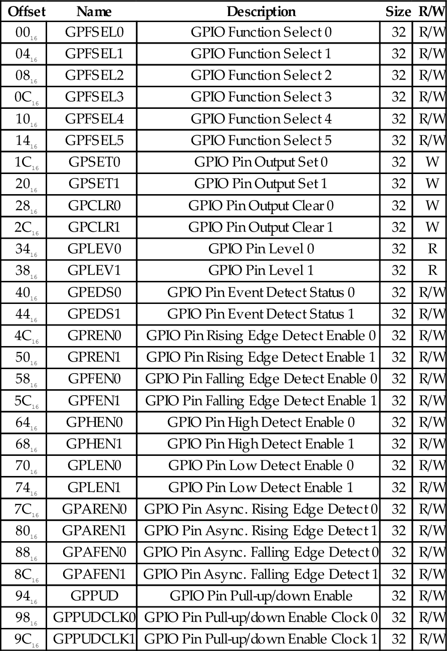
Setting the GPIO pin function
The first six 32-bit registers in the device are used to select the function for each of the 54 GPIO pins. The function of each pin is controlled by a group of three bits in one of these registers. The mapping is very regular. Bits 0–2 of GPIOFSEL0 control the function of GPIO pin 0. Bits 3–5 of GPIOFSEL0 control the function of GPIO pin 1, and so on, up to bits 27–29 of GPIOFSEL0, which control the function of GPIO pin 9. The next pin, pin 10, is controlled by bits 0–2 of GPIOFSEL1. The pins are assigned in sequence through the remaining bits, until bits 27–29, which control GPIO pin 19. The remaining four GPIOFSEL registers control the remaining GPIO pins. Note that bits 30 and 31 of all of the GPIOFSEL registers are not used, and most of the bits in GPIOFSEL5 are not assigned to any pin. The meaning of each combination of the three bits is shown in Table 11.2. Note that the encoding is not as simple as one might expect.
Table 11.2
GPIO pin function select bits
| MSB-LSB | Function |
| 000 | Pin is an input |
| 001 | Pin is an output |
| 100 | Pin performs alternate function 0 |
| 101 | Pin performs alternate function 1 |
| 110 | Pin performs alternate function 2 |
| 111 | Pin performs alternate function 3 |
| 011 | Pin performs alternate function 4 |
| 010 | Pin performs alternate function 5 |
The procedure for setting the function of a GPIO pin is as follows:
• Determine which GPIOFSEL register controls the desired pin.
• Determine which bits of the GPIOFSEL register are used.
• Determine what the bit pattern should be.
• Read the GPIOFSEL register.
• Clear the correct bits using the bic instruction.
• Set them to the correct pattern using the orr instruction.
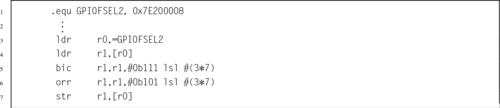
For example, Listing 11.3 shows the sequence of code which would be used to set GPIO pin 26 to alternate function 1.
Setting GPIO output pins
To use a GPIO pin for output, the function select bits for that pin must be set to 001. Once that is done, the output can be driven high or low by using the GPSET and GPCLR registers. GPIO pin 0 is set to a high output by writing a 1 to bit 0 of GPSET0, and it is set to low output by writing a 1 to bit 0 of GPCLR0. GPIO pin 1 is similarly controlled by bit 1 in GPSET0 and GPCLR0. Each of the GPIO pins numbered 0 through 31 is assigned one bit in GPSET0 and one bit in GPCLR0. GPIO pin 32 is assigned to bit 0 of GPSET1 and GPCLR1, GPIO pin 33 is assigned to bit 1 of GPSET1 and GPCLR1, and so on. Since there are only 54 GPIO pins, bits 22–31 of GPSET1 and GPCLR1 are not used. The programmer can set or clear several outputs simultaneously by writing the appropriate bits in the GPSET and GPCLR registers.
Reading GPIO input pins
To use a GPIO pin for input, the function select bits for that pin must be set to 000. Once that is done, the input can be read at any time by reading the appropriate GPLEV register and examining the bit that corresponds with the input pin. GPIO pin 0 is read as bit 0 of GPLEV0, GPIO pin 1 is similarly read as bit 1 of GPLEV1. Each of the GPIO pins numbered 0 through 31 is assigned one bit in GPLEV0. GPIO pin 32 is assigned to bit 0 of GPLEV1, GPIO pin 33 is assigned to bit 1 of GPLEV1, and so on. Since there are only 54 GPIO pins, bits 22–31 of GPLEV1 are not used. The programmer can read the status of several inputs simultaneously by reading one of the GPLEV registers and examining the bits corresponding to the appropriate pins.
Enabling internal pull-up or pull-down
Input pins can be configured with internal pull-up or pull-down resistors. This can simplify the design of the system. For instance, Fig. 11.2A, shows a push-button switch connected to an input, with an external pull-up resistor. That resistor is unnecessary if the internal pull-up for that pin is enabled.
Enabling the pull-up or pull-down is a two step process. The first step is to configure the type of change to be made, and the second step is to perform that change on the selected pin(s). The first step is accomplished by writing to the GPPUD register. The valid binary control codes are shown in Table 11.3.
Table 11.3
GPPUD control codes
| Code | Function |
| 00 | Disable pull-up and pull-down |
| 01 | Enable pull-down |
| 10 | Enable pull-up |
Once the GPPUD register is configured, the selected operation can be performed on multiple pins by writing to one or both of the GPPUDCLK registers. GPIO pins are assigned to bits in these two registers in the same way as the pins are assigned in the GPLEV, GPSET, and GPCLR registers. Writing 1 to bit 0 of GPPUDCLK0 will configure the pull-up or pull-down for GPIO pin 0, according to the control code that is currently in the GPPUD register.
Detecting GPIO events
The GPEDS registers are used for detecting events that have occurred on the GPIO pins. For instance a pin may have transitioned from low to high, and back to low. If the CPU does not read the GPLEV register often enough, then such an event could be missed. The GPEDS registers can be configured to capture such events so that the CPU can detect that they occurred.
GPIO pins are assigned to bits in these two registers in the same way as the pins are assigned in the GPLEV, GPSET, and GPCLR registers. If bit 1 of GPEDS0 is set, then that indicates that an event has occurred on GPIO pin 0. Writing a 0 to that bit will clear the bit and allow the event detector to detect another event. Each pin can be configured to detect specific types of events by writing to the GPREN, GPHEN, GPLEN, GPAREN, and GPAFEN registers. For more information, refer to the BCM2835 ARM Peripherals manual.
GPIO pins available on the Raspberry Pi
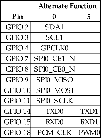
The Raspberry Pi provides access to several of the 54 GPIO pins through the expansion header. The expansion header is a group of physical pins located in the corner of the Raspberry Pi board. Fig. 11.3 shows where the header is located on the Raspberry Pi. Wires can be connected to these pins and then the GPIO device can be programmed to send and/or receive digital information. Fig. 11.4 shows which signals are attached to the various pins. Some of the pins are used to provide power and ground to the external devices.
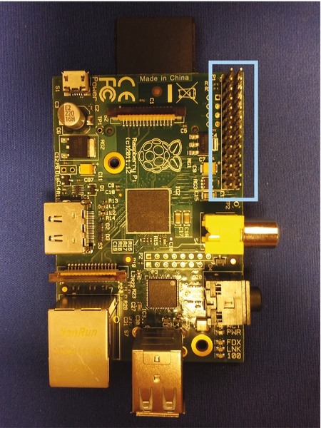
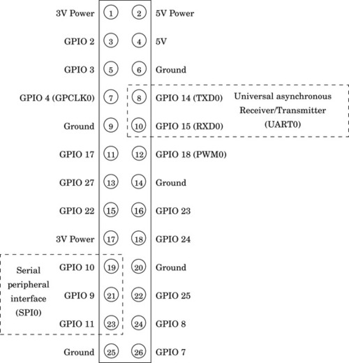
Table 11.4 shows some useful alternate functions available on each pin of the Raspberry Pi expansion header. Many of the alternate functions available on these pins are not really useful. Those functions have been left out of the table. The most useful alternate functions are probably GPIO 14 and 15, which can be used for serial communication, and GPIO 18, which can be used for pulse width modulation. Pulse width modulation is covered in Section 12.2, and serial communication is covered in Section 13.2. The Serial Peripheral Interface (SPI) functions could also be useful for connecting the Raspberry Pi to other devices which support SPI. Also, the SDA and SCL functions could be used to communicate with I2C devices.
11.2.2 pcDuino GPIO
The AllWinner A10/A20 system-on-chip contains 175 GPIO pins, which are arranged in seven ports. Each of the seven ports is identified by a letter between “A” and “I.” The ports are part of the PIO device, which is mapped at address 01C2080016. The GPIO pins are named using the following format: PNx, where N is a letter between “A” and “I” indicating the port, and x is a number indicating a pin on the given port. The assignment of pins to ports is somewhat irregular, as shown in Table 11.5. Some ports have as many as 28 physical pins, while others have as few as six. However, the layout of the registers in the device is very regular. Given any port and pin combination, finding the correct registers and sets of bits within the registers, is very straightforward.
Table 11.5
Number of pins available on each of the AllWinner A10/A20 PIO ports
| Port | Pins |
| A | 18 |
| B | 24 |
| C | 25 |
| D | 28 |
| E | 12 |
| F | 6 |
| G | 12 |
| H | 28 |
| I | 22 |
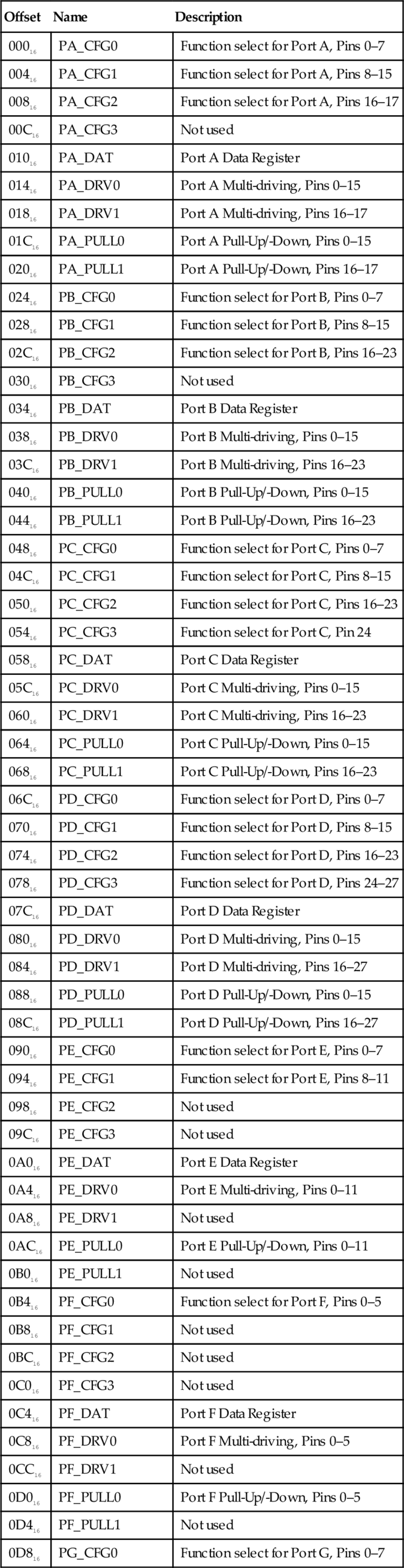
Each of the 9 ports is controlled by a set of 9 registers, for a total of 81 registers. There are seven additional registers that can be used to configure pins as interrupt sources. Interrupt processing is explained in Section 14.2. All of the port and interrupt registers together make a total of 88 registers for the GPIO device. The complete register map with the offset of each register from the device base address is shown in Table 11.6.
Table 11.6
Registers in the AllWinner GPIO device
| Offset | Name | Description |
| 00016 | PA_CFG0 | Function select for Port A, Pins 0–7 |
| 00416 | PA_CFG1 | Function select for Port A, Pins 8–15 |
| 00816 | PA_CFG2 | Function select for Port A, Pins 16–17 |
| 00C16 | PA_CFG3 | Not used |
| 01016 | PA_DAT | Port A Data Register |
| 01416 | PA_DRV0 | Port A Multi-driving, Pins 0–15 |
| 01816 | PA_DRV1 | Port A Multi-driving, Pins 16–17 |
| 01C16 | PA_PULL0 | Port A Pull-Up/-Down, Pins 0–15 |
| 02016 | PA_PULL1 | Port A Pull-Up/-Down, Pins 16–17 |
| 02416 | PB_CFG0 | Function select for Port B, Pins 0–7 |
| 02816 | PB_CFG1 | Function select for Port B, Pins 8–15 |
| 02C16 | PB_CFG2 | Function select for Port B, Pins 16–23 |
| 03016 | PB_CFG3 | Not used |
| 03416 | PB_DAT | Port B Data Register |
| 03816 | PB_DRV0 | Port B Multi-driving, Pins 0–15 |
| 03C16 | PB_DRV1 | Port B Multi-driving, Pins 16–23 |
| 04016 | PB_PULL0 | Port B Pull-Up/-Down, Pins 0–15 |
| 04416 | PB_PULL1 | Port B Pull-Up/-Down, Pins 16–23 |
| 04816 | PC_CFG0 | Function select for Port C, Pins 0–7 |
| 04C16 | PC_CFG1 | Function select for Port C, Pins 8–15 |
| 05016 | PC_CFG2 | Function select for Port C, Pins 16–23 |
| 05416 | PC_CFG3 | Function select for Port C, Pin 24 |
| 05816 | PC_DAT | Port C Data Register |
| 05C16 | PC_DRV0 | Port C Multi-driving, Pins 0–15 |
| 06016 | PC_DRV1 | Port C Multi-driving, Pins 16–23 |
| 06416 | PC_PULL0 | Port C Pull-Up/-Down, Pins 0–15 |
| 06816 | PC_PULL1 | Port C Pull-Up/-Down, Pins 16–23 |
| 06C16 | PD_CFG0 | Function select for Port D, Pins 0–7 |
| 07016 | PD_CFG1 | Function select for Port D, Pins 8–15 |
| 07416 | PD_CFG2 | Function select for Port D, Pins 16–23 |
| 07816 | PD_CFG3 | Function select for Port D, Pins 24–27 |
| 07C16 | PD_DAT | Port D Data Register |
| 08016 | PD_DRV0 | Port D Multi-driving, Pins 0–15 |
| 08416 | PD_DRV1 | Port D Multi-driving, Pins 16–27 |
| 08816 | PD_PULL0 | Port D Pull-Up/-Down, Pins 0–15 |
| 08C16 | PD_PULL1 | Port D Pull-Up/-Down, Pins 16–27 |
| 09016 | PE_CFG0 | Function select for Port E, Pins 0–7 |
| 09416 | PE_CFG1 | Function select for Port E, Pins 8–11 |
| 09816 | PE_CFG2 | Not used |
| 09C16 | PE_CFG3 | Not used |
| 0A016 | PE_DAT | Port E Data Register |
| 0A416 | PE_DRV0 | Port E Multi-driving, Pins 0–11 |
| 0A816 | PE_DRV1 | Not used |
| 0AC16 | PE_PULL0 | Port E Pull-Up/-Down, Pins 0–11 |
| 0B016 | PE_PULL1 | Not used |
| 0B416 | PF_CFG0 | Function select for Port F, Pins 0–5 |
| 0B816 | PF_CFG1 | Not used |
| 0BC16 | PF_CFG2 | Not used |
| 0C016 | PF_CFG3 | Not used |
| 0C416 | PF_DAT | Port F Data Register |
| 0C816 | PF_DRV0 | Port F Multi-driving, Pins 0–5 |
| 0CC16 | PF_DRV1 | Not used |
| 0D016 | PF_PULL0 | Port F Pull-Up/-Down, Pins 0–5 |
| 0D416 | PF_PULL1 | Not used |
| 0D816 | PG_CFG0 | Function select for Port G, Pins 0–7 |
| 0DC16 | PG_CFG1 | Function select for Port G, Pins 8–11 |
| 0E016 | PG_CFG2 | Not used |
| 0E416 | PG_CFG3 | Not used |
| 0E816 | PG_DAT | Port G Data Register |
| 0EC16 | PG_DRV0 | Port G Multi-driving, Pins 0–11 |
| 0F016 | PG_DRV1 | Not used |
| 0F416 | PG_PULL0 | Port G Pull-Up/-Down, Pins 0–11 |
| 0F816 | PG_PULL1 | Not used |
| 0FC16 | PH_CFG0 | Function select for Port H, Pins 0–7 |
| 10016 | PH_CFG1 | Function select for Port H, Pins 8–15 |
| 10416 | PH_CFG2 | Function select for Port H, Pins 16–23 |
| 10816 | PH_CFG3 | Function select for Port H, Pins 24–27 |
| 10C 16 | PH_DAT | Port H Data Register |
| 11016 | PH_DRV0 | Port H Multi-driving, Pins 0–15 |
| 11416 | PH_DRV1 | Port H Multi-driving, Pins 16–27 |
| 11816 | PH_PULL0 | Port H Pull-Up/-Down, Pins 0–15 |
| 11C16 | PH_PULL1 | Port H Pull-Up/-Down, Pins 16–27 |
| 12016 | PI_CFG0 | Function select for Port I, Pins 0–7 |
| 12416 | PI_CFG1 | Function select for Port I, Pins 8–15 |
| 12816 | PI_CFG2 | Function select for Port I, Pins 16–21 |
| 12C16 | PI_CFG3 | Not used |
| 13016 | PI_DAT | Port I Data Register |
| 13416 | PI_DRV0 | Port I Multi-driving, Pins 0–15 |
| 13816 | PI_DRV1 | Port I Multi-driving, Pins 16–21 |
| 13C16 | PI_PULL0 | Port I Pull-Up/-Down, Pins 0–15 |
| 14016 | PI_PULL1 | Port I Pull-Up/-Down, Pins 16–21 |
| 20016 | PIO_INT_CFG0 | PIO Interrupt Configure Register 0 |
| 20416 | PIO_INT_CFG1 | PIO Interrupt Configure Register 1 |
| 20816 | PIO_INT_CFG2 | PIO Interrupt Configure Register 2 |
| 20C16 | PIO_INT_CFG3 | PIO Interrupt Configure Register 3 |
| 21016 | PIO_INT_CTL | PIO Interrupt Control Register |
| 21416 | PIO_INT_STATUS | PIO Interrupt Status Register |
| 21816 | PIO_INT_DEB | PIO Interrupt Debounce Register |
The GPIO pins are highly configurable. Each pin can be used either for general purpose I/O, or can be configured to serve one of up to six pre-defined alternate functions. Configuring a GPIO pin for an alternate function usually allows some other device within the A10/A20 SOC to use the pin. For example PB2 (pin 2 of port B) can be used for general purpose I/O, or can be used to output the signal from a Pulse Width Modulator (PWM) device (explained in Section 12.2). Each input pin also has internal pull-up and pull-down resistors, which can be enabled or disabled by the programmer.
Setting the GPIO pin function
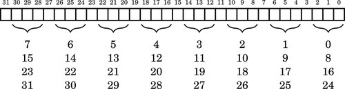
The first four registers for each port are used to configure the functions for each of the pins. The function of each pin is controlled by three bits in one of the four configuration registers. Pins 0–7 are controlled using configuration register 0. Pins 8–15 are controlled by configuration register 1, and so on. The assignment of pins to control bits is shown in Fig. 11.5. Note that eight pins are controlled by each register, and there is an unused bit between each group of three bits.
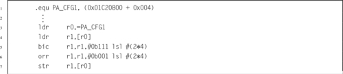
Each GPIO pin can be configured by writing a 3-bit code to the appropriate location in the correct port configuration register. The meanings of each possible code is shown in Table 11.7. For example, to configure port A, pin 10 (PA10) for output, the 3-bit code 001 must be written to bits 8–10 the PA_CFG1 register, without changing any other bit in the register. Listing 11.4 shows how this operation can be accomplished.
Table 11.7
Allwinner A10/A20 GPIO pin function select bits
| MSB-LSB | Function |
| 000 | Pin is an input |
| 001 | Pin is an output |
| 010 | Pin performs alternate function 0 |
| 011 | Pin performs alternate function 1 |
| 100 | Pin performs alternate function 2 |
| 101 | Pin performs alternate function 3 |
| 110 | Pin performs alternate function 4 |
| 111 | Pin performs alternate function 5 |
Reading and setting GPIO pins
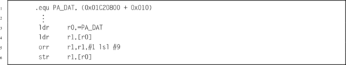
An output pin can be set to a high state by setting the corresponding bit in the correct port data register. Likewise the pin can be set to a low state by clearing its corresponding bit. Care must be taken to avoid changing any other bits in the port data register. Listing 11.5 shows how this operation can be accomplished for setting a port to output a high state. To set the port output to a low state, the orr instruction would be replaced with a bic instruction.
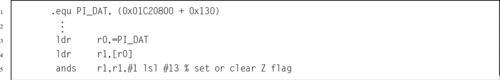
To determine the current state of an output pin or read an input pin, the programmer can read the contents of the correct port data register and use bitwise logical operations to isolate the appropriate bit. For example, to read the state of pin 14 of port I (PI14), the programmer would read the PI_DAT register and mask all bits except bit 14. Listing 11.6 shows how this operation can be accomplished. Another method would be to use the tst instruction, rather than the ands instruction, to set the CPSR flags.
Enabling internal pull-up or pull-down
Input pins can be configured with internal pull-up or pull-down resistors. This can simplify the design of the system. For instance, Fig. 11.2a, shows a push-button switch connected to an input with an external pull-up resistor. That resistor is unnecessary if the internal pull-up for that pin is enabled. Each pin is assigned two bits in one of the port pull-up/-down registers. The pull-up and pull-down resistors for pin 0 on port B are controlled using bits 0 and 1 of the PB_PULL0 register. Likewise the pull-up and pull-down resistors for pin 19 of port C are controlled using bits 6 and 7 of the PC_PULL1 register. Table 11.8 shows the bit patterns used to configure the pull-up and pull-down resisters for a pin.
Detecting GPIO events
When configured as an input, most of the pins on the pdDuino can be configured to generate an interrupt, which notifies the CPU than an event has occurred. Configuration of interrupts is beyond the scope of this chapter. It is accomplished using the PIO_INT registers.
GPIO pins available on the pcDuino
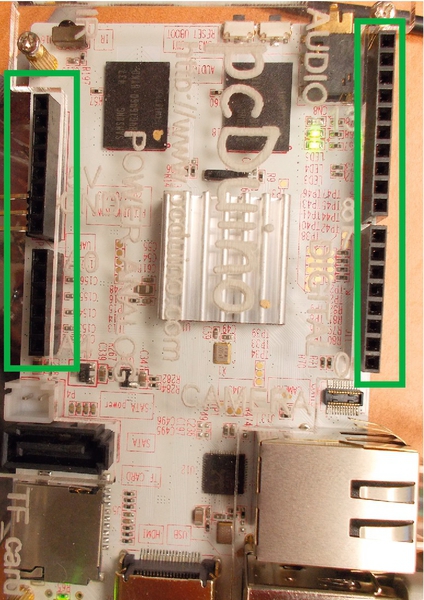
The pcDuino provides access to several of the 175 GPIO pins through the expansion headers. Fig. 11.6 shows where the headers are located on the pcDuino. Wires can be plugged into the holes in these headers and then the GPIO device can be programmed to send and/or receive digital and/or analog signals. The physical layout of the pcDuino header makes it compatible with a wide range of expansion modules designed for the Arduino family of microcontroller boards.
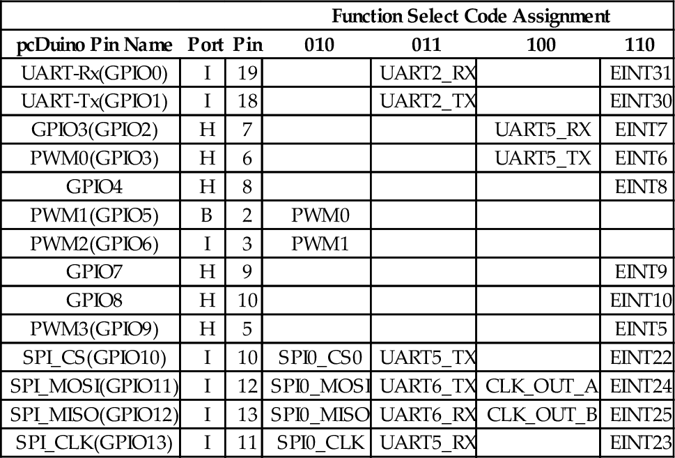
Some of the header holes can provide power and ground to the external devices. Analog signals can be read into the pcDuino using the ADC header connections. Fig. 11.7 shows the pcDuino names for the signals that are available on the headers. Table 11.9 shows how the pcDuino header signal names are mapped to the actual port pins on the AllWinner A10/A20 chip. It also shows the most useful alternate functions available on each of the pins. Many alternate functions are left out of the table because they are not really useful. Note that the pcDunio and the Raspberry Pi both provide pins to perform PWM, UART communications, and SPI.
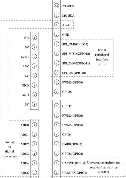
Table 11.9
pcDuino GPIO pins and function select code assignments.
| Function Select Code Assignment | ||||||
| pcDuino Pin Name | Port | Pin | 010 | 011 | 100 | 110 |
| UART-Rx(GPIO0) | I | 19 | UART2_RX | EINT31 | ||
| UART-Tx(GPIO1) | I | 18 | UART2_TX | EINT30 | ||
| GPIO3(GPIO2) | H | 7 | UART5_RX | EINT7 | ||
| PWM0(GPIO3) | H | 6 | UART5_TX | EINT6 | ||
| GPIO4 | H | 8 | EINT8 | |||
| PWM1(GPIO5) | B | 2 | PWM0 | |||
| PWM2(GPIO6) | I | 3 | PWM1 | |||
| GPIO7 | H | 9 | EINT9 | |||
| GPIO8 | H | 10 | EINT10 | |||
| PWM3(GPIO9) | H | 5 | EINT5 | |||
| SPI_CS(GPIO10) | I | 10 | SPI0_CS0 | UART5_TX | EINT22 | |
| SPI_MOSI(GPIO11) | I | 12 | SPI0_MOSI | UART6_TX | CLK_OUT_A | EINT24 |
| SPI_MISO(GPIO12) | I | 13 | SPI0_MISO | UART6_RX | CLK_OUT_B | EINT25 |
| SPI_CLK(GPIO13) | I | 11 | SPI0_CLK | UART5_RX | EINT23 | |
11.3 Chapter Summary
All input and output are accomplished by using devices. There are many types of devices, and each device has its own set of registers which are used to control the device. The programmer must understand the operation of the device and the use of each register in order to use the device at a low level. Computer system manufacturers usually can provide documentation providing the necessary information for low-level programming. The quality of the documentation can vary greatly, and a general understanding of various types of devices can help in deciphering poor or incomplete documentation.
There are two major tasks where programming devices at the register level is required: operating system drivers and very small embedded systems. Operating systems provide an abstract view of each device and this allows programmers to use them more easily. However, someone must write that driver, and that person must have intimate knowledge of the device. On very small systems, there may not be a driver available. In that case, the device must be accessed directly. Even when an operating system provides a driver, it is sometimes necessary or desirable for the programmer to access the device directly. For example, some devices may provide modes of operation or capabilities that are not supported by the operating system driver. Linux provides a mechanism which allows the programmer to map a physical device into the program’s memory space, thereby gaining access to the raw device registers.
Exercises
11.1 Explain the relationships and differences between device registers, memory locations, and CPU registers.
11.2 Why is it necessary to map the device into user program memory before accessing it under Linux? Would this step be necessary under all operating systems or in the case where there is no operating system and our code is running on the “bare metal?”
11.3 What is the purpose of a GPIO device?
11.4 The Raspberry Pi and the PcDuino have very different GPIO devices.
(a) Are they functionally equivalent?
(b) Are they equally programmer-friendly?
(c) If you have answered no to either of the previous questions, then what are the differences?
11.5 Draw a circuit diagram showing how to connect:
(a) a pushbutton switch to GPIO 23 and an LED to GPIO 27 on the Raspberry Pi, and
(b) a pushbutton switch to GPIO12 and an LED to GPIO13 on the PcDuino.
11.6 Assuming the systems are wired according to the previous exercise, write two functions. One function must initialize the GPIO pins, and the other function must read the state of the switch and turn the LED on if the button is pressed, and off if the button is not pressed. Write the two functions for
(b) a PcDuino.
11.7 Write the code necessary to route the output from PWM0 to GPIO 18 on a Raspberry Pi.
11.8 Write the code necessary to route the output from PWM0 to GPIO 5 on a PcDuino.