Table of Contents for
Modern Assembly Language Programming with the ARM Processor
 Modern Assembly Language Programming with the ARM Processor
Published by
Newnes, 2016
Modern Assembly Language Programming with the ARM Processor
Published by
Newnes, 2016
- Modern Assembly Language Programming with the ARM Processor
- Cover image
- Title page
- Table of Contents
- Copyright
- List of Tables
- List of Figures
- List of Listings
- Preface
- Companion Website
- Acknowledgments
- Part I: Assembly as a Language
- Chapter 1: Introduction
- Chapter 2: GNU Assembly Syntax
- Chapter 3: Load/Store and Branch Instructions
- Chapter 4: Data Processing and Other Instructions
- Chapter 5: Structured Programming
- Chapter 6: Abstract Data Types
- Part II: Performance Mathematics
- Chapter 7: Integer Mathematics
- Chapter 8: Non-Integral Mathematics
- Chapter 9: The ARM Vector Floating Point Coprocessor
- Chapter 10: The ARM NEON Extensions
- 10.10 Multiplication and Division
- Part III: Accessing Devices
- Chapter 11: Devices
- Chapter 12: Pulse Modulation
- Chapter 13: Common System Devices
- Chapter 14: Running Without an Operating System
- Index
Pulse Modulation
Abstract
This chapter begins by explaining pulse density and pulse width modulation in general terms. It then introduces and describes the PWM device on the Raspberry Pi. Following that, it covers the pcDuino PWM device. This gives the reader another opportunity to see two different devices which both perform essentially the same functions.
Keywords
Pulse width modulation; Pulse density modulation; Digital to analog; Low pass filter
The GPIO device provides a method for sending digital signals to external devices. This can be useful to control devices that have basically two states: on and off. In some situations, it is useful to have the ability to turn a device on at varying levels. For instance, it could be useful to control a motor at any required speed, or control the brightness of a light source. One way that this can be accomplished is through pulse modulation.
The basic idea is that the computer sends a stream of pulses to the device. The device acts as a low-pass filter, which averages the digital pulses into an analog voltage. By varying the percentage of time that the pulses are high, versus low, the computer can control how much average energy is sent to the device. The percentage of time that the pulses are high versus low is known as the duty cycle. Varying the duty cycle is referred to as modulation. There are two major types of pulse modulation: pulse density modulation (PDM) and pulse width modulation (PWM). Most pulse modulation devices are configured in three steps as follows:
1. The base frequency of the clock that drives the PWM device is configured. This step is usually optional.
2. The mode of operation for the pulse modulation device is configured by writing to one or more configuration registers in the pulse modulation device.
3. The cycle time is set by writing a “range” value into a register in the pulse modulation device. This value is usually set as a multiple of the base clock cycle time.
Once the device is configured, the duty cycle can be changed easily by writing to one or more registers in the pulse modulation device.
12.1 Pulse Density Modulation
With PDM, also known as pulse frequency modulation (PFM), the duration of the positive pulses does not change, but the time between them (the pulse density) is modulated. When using PDM devices, the programmer typically sets the device cycle time tc in a register, then uses another register to specify the number of pulses d that are to be sent during a device cycle. The number of pulses is typically referred to as the duty cycle and must be chosen such that 0 ≤ d ≤ tc. For instance, if tc = 1024, then the device cycle time is 1024 times the cycle time of the clock that drives the device. If d = 512, then the device will send 512 pulses, evenly spaced, during the device cycle. Each pulse will have the same duration as the base clock. The device will continue to output this pulse pattern until d is changed.
Fig. 12.1 shows a signal that is being sent using PDM, and the resulting set of pulses. Each pulse transfers a fixed amount of energy to the device. When the pulses arrive at the device, they are effectively filtered using a low pass filter. The resulting received signal is also shown. Notice that the received signal has a delay, or phase shift, caused by the low-pass filtering. This approach is suitable for controlling certain types of devices, such as lights and speakers.
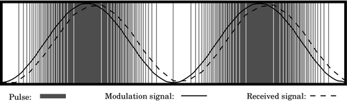
However, when driving such devices directly with the digital pulses, care must be taken that the minimum frequency of pulses remains above the threshold that can be detected by human senses. For instance, when driving a speaker, the minimum pulse frequency must be high enough that the individual pulses cannot be distinguished by the human ear. This minimum frequency is around 40 kHz. Likewise, when driving an LED directly, the minimum frequency must be high enough that the eye cannot detect the individual pulses, because they will be seen as a flickering effect. That minimum frequency is around 70 Hz. To reduce or alleviate this problem, designers may add a low-pass filter between the PWM device and the device that is being driven.
12.2 Pulse Width Modulation
In PWM, the frequency of the pulses remains fixed, but the duration of the positive pulse (the pulse width) is modulated. When using PWM devices, the programmer typically sets the device cycle time tc in a register, then uses another register to specify the number of base clock cycles, d, for which the output should be high. The percentage  is typically referred to as the duty cycle and d must be chosen such that 0 ≤ d ≤ tc. For instance, if tc = 1024, then the device cycle time is 1024 times the cycle time of the clock that drives the device. If d = 512, then the device will output a high signal for 512 clock cycles, then output a low signal for 512 clock cycles. It will continue to repeat this pattern of pulses until d is changed.
Fig. 12.2 shows a signal that is being sent using PWM. The pulses are also shown. Each pulse transfers some energy to the device. The width of each pulse determines how much energy is transferred. When the pulses arrive at the device, they are effectively filtered using a low-pass filter. The resulting received signal is shown by the dashed line. As with PDM, the received signal has a delay, or phase shift, caused by the low-pass filtering.
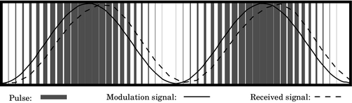
One advantage of PWM over PDM is that the digital circuit is not as complex. Another advantage of PWM over PDM is that the frequency of the pulses does not vary, so it is easier for the programmer to set the base frequency high enough that the individual pulses cannot be detected by human senses. Also, when driving motors it is usually necessary to match the pulse frequency to the size and type of motor. Mismatching the frequency can cause loss of efficiency as well as overheating of the motor and drive electronics. In severe cases, this can cause premature failure of the motor and/or drive electronics. With PWM, it is easier for the programmer to control the base frequency, and thereby avoid those problems.
12.3 Raspberry Pi PWM Device
The Broadcom BCM2835 system-on-chip includes a device that can create two PWM signals. One of the signals (PWM0) can be routed through GPIO pin 18 (alternate function 5), where it is available on the Raspberry Pi expansion header at pin 12. PWM0 can also be routed through GPIO pin 40. On the Raspberry Pi, pin 40 it is sent through a low-pass filter, and then to the Raspberry Pi audio output port as the right stereo channel. The other signal (PWM1) can be routed through GPIO pin 45. From there, it is sent through a low-pass filter, and then to the Raspberry Pi audio output port as the left stereo channel. So, both PWM channels are accessible, but PWM1 is only accessible through the audio output port after it has been low-pass filtered. The raw PWM0 signal is available through the Raspberry Pi expansion header at pin 12.
There are three modes of operation for the BCM2835 PWM device:
2. PWM mode, and
3. serial transmission mode.
The following paragraphs explain how the device can be used in basic PWM mode, which is the most simple and straightforward mode for this device. Information on how to use the PDM and serial transmission modes, the FIFO, and DMA is available in the BCM2835 ARM Peripherals manual.
The base address of the PWM device is 2020C00016 and it contains eight registers. Table 12.1 shows the offset, name, and a short description for each of the registers. The mode of operation is selected for each channel independently by writing appropriate bits in the PWMCTL register. The base clock frequency is controlled by the clock manager device, which is explained in Section 13.1. By default, the system startup code sets the base clock for the PWM device to 100 MHz.
Table 12.1
Raspberry Pi PWM register map
| Offset | Name | Description | Size | R/W |
| 0016 | PWMCTL | PWM Control | 32 | R/W |
| 0416 | PWMSTA | PWM FIFO Status | 32 | R/W |
| 0816 | PWMDMAC | PWM DMA Configuration | 32 | R/W |
| 1016 | PWMRNG1 | PWM Channel 1 Range | 32 | R/W |
| 1416 | PWMDAT1 | PWM Channel 1 Data | 32 | R/W |
| 1816 | PWMFIF1 | PWM FIFO Input | 32 | R/W |
| 2016 | PWMRNG2 | PWM Channel 2 Range | 32 | R/W |
| 2416 | PWMDAT2 | PWM Channel 2 Data | 32 | R/W |
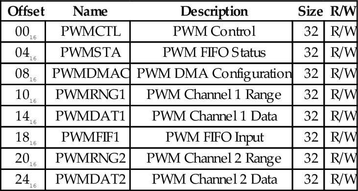
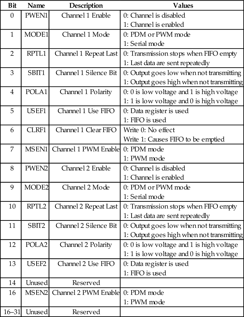
Table 12.2 shows the names and short descriptions of the bits in the PWMCTL register. There are 8 bits used for controlling channel 1 and 8 bits for controlling channel 2. PWENn is the master enable bit for channel n. Setting that bit to 0 disables the PWM channel, while setting it to 1 enables the channel. MODEn is used to select whether the channel is in serial transmission mode or in the PDM/PWM mode. If MODEn is set to 0, then MSENn is used to choose whether channel n is in PDM mode or PWM mode. If MODEn is set to 1, then RPTLn, SBITn, USEFn, and CLRFn are used to manage the operation of the FIFO for channel n. POLAn is used to enable or disable inversion of the output signal for channel n.
Table 12.2
Raspberry Pi PWM control register bits
The PWMRNGn registers are used to define the base period for the corresponding channel. In PDM mode, evenly distributed pulses are sent within a period of length defined by this register, and the number of pulses sent during the base period is controlled by writing to the corresponding PWMDATn register. In PWM mode, the PWMRNGn register defines the base frequency for the pulses, and the duty cycle is controlled by writing to the corresponding PWMDATn register. Example 12.1 gives an overview of the steps needed to configure PWM0 for use in PWM mode.
12.4 pcDuino PWM Device
The AllWinner A10/A20 SOCs have a hardware PWM device which is capable of generating two PWM signals. The PWM device is driven by the OSC24M signal, which is generated by the Clock Control Unit (CCU) in the AllWinner SOC. This base clock runs at 24 MHz by default, and changing the base frequency could affect many other devices in the system. The base clock can be divided by one of 11 predefined values using a prescaler built into the PWM device. Each of the two channels has its own prescaler. Table 12.3 shows the possible settings for the prescalers.
Table 12.3
Prescaler bits in the pcDuino PWM device
| Value | Effect |
| 0000 | Base clock is divided by 120 |
| 0001 | Base clock is divided by 180 |
| 0010 | Base clock is divided by 240 |
| 0011 | Base clock is divided by 360 |
| 0100 | Base clock is divided by 480 |
| 0101,0110,0111 | Not used |
| 1000 | Base clock is divided by 1200 |
| 1001 | Base clock is divided by 2400 |
| 1010 | Base clock is divided by 3600 |
| 1011 | Base clock is divided by 4800 |
| 1100 | Base clock is divided by 7200 |
| 1101,1110 | Not used |
| 1111 | Base clock is divided by 1 |
There are two modes of operation for the PWM device. In the first mode, the device operates like a standard PWM device as described in Section 12.2. In the second mode, it sends a single pulse and then waits until it is triggered again by the CPU. In this mode, it is a monostable multivibrator, also known as a one-shot multivibrator, or just one-shot. The duration of the pulse is controlled using the pre-scaler and the period register.
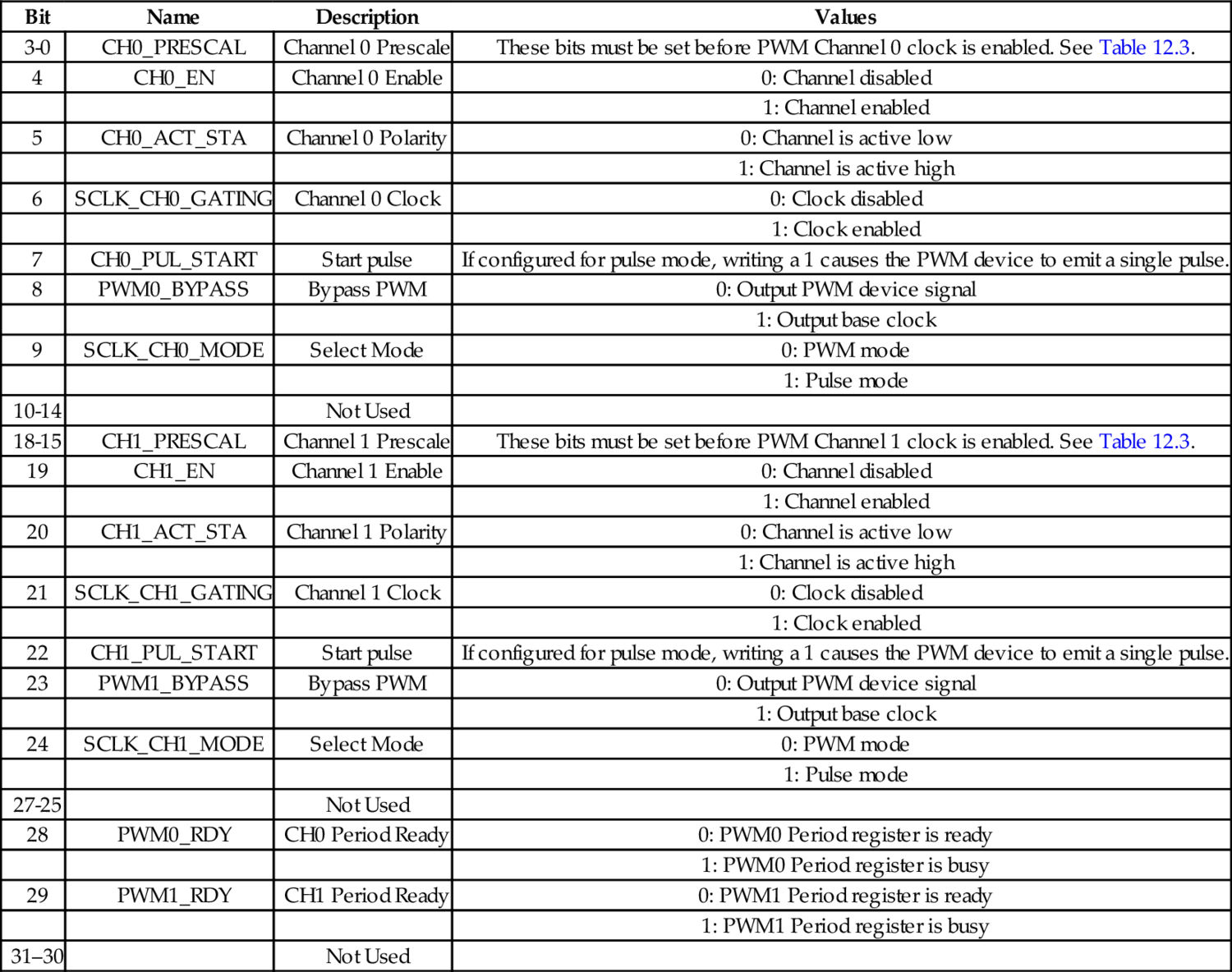
The PWM device is mapped at address 01C20C0016. Table 12.4 shows the registers and their offsets from the base address. All of the device configuration is done through a single control register, which can also be read in order to determine the status of the device. The bits in the control register are shown in Table 12.5.
Table 12.4
pcDuino PWM register map
| Offset | Name | Description |
| 20016 | PWMCTL | PWM Control |
| 20416 | PWM_CH0_PERIOD | PWM Channel 0 Period |
| 20816 | PWM_CH1_PERIOD | PWM Channel 1 Period |
Table 12.5
pcDuino PWM control register bits
| Bit | Name | Description | Values |
| 3-0 | CH0_PRESCAL | Channel 0 Prescale | These bits must be set before PWM Channel 0 clock is enabled. See Table 12.3. |
| 4 | CH0_EN | Channel 0 Enable | 0: Channel disabled |
| 1: Channel enabled | |||
| 5 | CH0_ACT_STA | Channel 0 Polarity | 0: Channel is active low |
| 1: Channel is active high | |||
| 6 | SCLK_CH0_GATING | Channel 0 Clock | 0: Clock disabled |
| 1: Clock enabled | |||
| 7 | CH0_PUL_START | Start pulse | If configured for pulse mode, writing a 1 causes the PWM device to emit a single pulse. |
| 8 | PWM0_BYPASS | Bypass PWM | 0: Output PWM device signal |
| 1: Output base clock | |||
| 9 | SCLK_CH0_MODE | Select Mode | 0: PWM mode |
| 1: Pulse mode | |||
| 10-14 | Not Used | ||
| 18-15 | CH1_PRESCAL | Channel 1 Prescale | These bits must be set before PWM Channel 1 clock is enabled. See Table 12.3. |
| 19 | CH1_EN | Channel 1 Enable | 0: Channel disabled |
| 1: Channel enabled | |||
| 20 | CH1_ACT_STA | Channel 1 Polarity | 0: Channel is active low |
| 1: Channel is active high | |||
| 21 | SCLK_CH1_GATING | Channel 1 Clock | 0: Clock disabled |
| 1: Clock enabled | |||
| 22 | CH1_PUL_START | Start pulse | If configured for pulse mode, writing a 1 causes the PWM device to emit a single pulse. |
| 23 | PWM1_BYPASS | Bypass PWM | 0: Output PWM device signal |
| 1: Output base clock | |||
| 24 | SCLK_CH1_MODE | Select Mode | 0: PWM mode |
| 1: Pulse mode | |||
| 27-25 | Not Used | ||
| 28 | PWM0_RDY | CH0 Period Ready | 0: PWM0 Period register is ready |
| 1: PWM0 Period register is busy | |||
| 29 | PWM1_RDY | CH1 Period Ready | 0: PWM1 Period register is ready |
| 1: PWM1 Period register is busy | |||
| 31–30 | Not Used |
Before enabling a PWM channel, the period register for that channel should be initialized. The two period registers are each organized as two 16-bit numbers. The upper 16 bits control the total number of clock cycles in one period. In other words, they control the base frequency of the PWM signal. The PWM frequency is calculated as
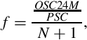
where OSC24M is the frequency of the base clock (the default is 24 MHz), PSC is the prescale value set in the channel prescale bits in the PWM control register, and N is the value stored in the upper 16 bits of the channel period register.
The lower 16 bits of the channel period register control the duty cycle. The duty cycle (expressed as % of full on) can be calculated as
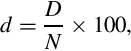
where N is the value stored in the upper 16 bits of the channel period register, and D is the value stored in the lower 16 bits of the channel period register. Note that the condition D ≤ N must always remain true. If the programmer allows D to become greater than N, the results are unpredictable.
The procedure for configuring the AllWinner A10/A20 PWM device is as follows:
1. Disable the desired channel:
(a) Read the PWM control register into x.
(b) Clear all of the bits in x for the desired PWM channel.
(c) Write x back to the PWM control register
2. Initialize the period register for the desired channel.
(a) Calculate the desired value for N.
(b) Let D = 0.
(c) Let y = N × 216 + D.
(d) Write y to the desired channel period register.
3. Set the prescaler.
(a) Select the four-bit code for the desired divisor from Table 12.3.
(b) Set the prescaler code bits in x.
(c) Write x back to the PWM control register.
4. Enable the PWM device.
(a) Set the appropriate bits in x to enable the desired channel, select the polarity, and enable the clock.
(b) Write x to the PWM control register.
Once the control register is configured, the duty cycle can be controlled by calculating a new value for D and then writing y = N × 216 + D to the desired channel period register.
12.5 Chapter Summary
Pulse modulation is a group of methods for generating analog signals using digital equipment, and is commonly used in control systems to regulate the power sent to motors and other devices. Pulse modulation techniques can have very low power loss compared to other methods of controlling analog devices, and the circuitry required is relatively simple.
The cycle frequency must be programmed to match the application. Typically, 10 Hz is adequate for controlling an electric heating element, while 120 Hz would be more appropriate for controlling an incandescent light bulb. Large electric motors may be controlled with a cycle frequency as low as 100 Hz, while smaller motors may need frequencies around 10,000 Hz. It can take some experimentation to find the best frequency for any given application.
Exercises
12.1 Write ARM assembly programs to configure PWM0 and the GPIO device to send a signal out on Raspberry Pi header pin 12 with:
(a) period of 1 ms and duty cycle of 25%, and
(b) frequency of 150 Hz and duty cycle of 63%.
12.2 Write ARM assembly programs to configure PWM0 and the GPIO device to send a signal out on the pcDuino PWM1/GPIO5 pin with:
(a) period of 1 ms and duty cycle of 25%, and
(b) frequency of 150 Hz and duty cycle of 63%.