Table of Contents for
X86 Assembly Language and C Fundamentals
 X86 Assembly Language and C Fundamentals
Published by
CRC Press, 2015
X86 Assembly Language and C Fundamentals
Published by
CRC Press, 2015
- X86 Assembly Language and C Fundamentals
- Preliminaries
- By the same Author
- X86 Assembly Language and C Fundamentals
- X86 Assembly Language and C Fundamentals
- Preface
- Chapter 1 Number Systems and Number Representations
- Chapter 2 X86 Processor Architecture
- Chapter 3 Addressing Modes
- Chapter 4 C Programming Fundamentals
- Chapter 5 Data Transfer Instructions
- Chapter 6 Branching and Looping Instructions
- Chapter 7 Stack Operations
- Chapter 8 Logical, Bit, Shift, and Rotate Instructions
- Chapter 9 Fixed-Point Arithmetic Instructions
- Chapter 10 Binary-Coded Decimal Arithmetic Instructions
- Chapter 11 Floating-Point Arithmetic Instructions
- Chapter 12 Procedures
- Chapter 13 String Instructions
- Chapter 14 Arrays
- Chapter 15 Macros
- Chapter 16 Interrupts and Input/Output Operations
- Chapter 17 Additional Programming Examples
- Appendix A ASCII Character Codes
- Appendix B Answers to Select Problems
Chapter 2
X86 Processor Architecture
Microprocessors have evolved considerably over the past four decades, from the Intel 4-bit 4004 to the multi-core processors of today. A multi-core processor consists of two or more separate central processing units (CPUs), called cores. Thus, a quad-core processor consists of four independent CPUs. Multi-core processors can be designed to accommodate very-long-instruction-words (VLIWs), a pipelined reduced-instruction-set computer (RISC), or as a vector processor that operates on sets or vectors. Multi-core processors are designed to operate with multiple threads; that is, to execute multiple tasks simultaneously. Multithreading takes advantage of memory latency in order to improve system performance.
The speed of computers has increased significantly with the advent of multi-core processing and multithreading. IBM recently announced the development of a supercomputer to operate at 20 petaflops; that is, 20 × 1015 floating-point operations per second, but this will undoubtedly be surpassed in the near future. Pipelined RISC processors also increase machine performance by increasing parallelism by fetching, decoding, and executing instructions simultaneously in a multi-stage pipeline.
2.1 General Architecture
All computers have the generic architecture shown in Figure 2.1. This figure does not apply to any specific machine, but is common to all computers. Since there are over twenty different X86 architectures, it would be unreasonable to illustrate all of the architectural variations in this section. Figure 2.1 will be expanded in a subsequent section to more appropriately correspond to the X86 architecture execution environment, including the different sets of registers. A computer has five main functional units: the arithmetic and logic unit (ALU); the control unit (or sequencer), both of which constitute the CPU; the storage unit comprising the main memory and cache; the input devices; and the output devices. The word memory will be used throughout the book, although the International Standards Organization (ISO) states that the word memory is a deprecated term for main storage, because memory is a human characteristic. However, the word memory is used almost exclusively throughout the computer industry.
2.2 Arithmetic and Logic Unit
The ALU may consist of a complex-instruction-set computer (CISC), a parallel processor, a pipelined reduced-instruction-set computer (RISC), or any other processor architecture. For a pipelined computer, there are many different stages in a pipeline, with each stage performing one unique operation in the instruction processing. When the pipeline is full, a result is obtained usually every clock cycle.
An example of a simple 4-stage pipeline is shown in Figure 2.2. The Ifetch stage fetches the instruction from memory; the Decode stage decodes the instruction and fetches the operands; the Execute stage performs the operation specified in the instruction; the Store stage stores the result in the destination location. The destination is a register file or a reorder queue if instructions are executed out of order. Four instructions are in progress at any given clock cycle. Each stage of the pipeline performs its task in parallel with all other stages.
If the instruction required is not available in the cache, then a cache miss occurs, necessitating a fetch from main memory. This is referred to as a pipeline stall and delays processing the next instruction. Information is passed from one stage to the next by means of a storage buffer, as shown in Figure 2.3. There must be a register in the input of each stage (or between stages) to store information that is transmitted from the preceding stage. This prevents data being processed by one stage from interfering with the following stage during the same clock period.
The ALU performs arithmetic operations, such as add, subtract, multiply, and divide in fixed-point, decimal, and floating-point number representations; increment and decrement; logical operations, such as AND, OR, NOT, exclusive-OR, exclusive-NOR; shifting operations, such as shift right algebraic (SRA), shift right logical (SRL), shift left algebraic (SLA), and shift left logical (SLL); and rotate operations, such as rotate right and rotate left.
2.3 Control Unit
The control unit, or control store, is part of the CPU and contains the microprogram, also referred to as microcode. The microprogram is stored in a high-speed memory and accommodates a set of low-level instructions that control the machine's hardware and is machine dependent; that is, it is written for a particular type computer. The instructions in a microprogram represent micro operations that the CPU performs to execute a machine-language instruction. A microprogram is also referred to as firmware.
A control word in the microprogram is normally a very-long instruction word (VLIW) — ten bytes or more — to perform the many micro operations required by a CPU instruction, such as effective address generation and load/reset registers. There are two types of control units: hardwired and microprogrammed. A Hardwired control unit is too complex for large machines and is inherently inflexible to changes required by design changes or modification of the instruction set. A microprogrammed control unit does not have the limitations of a hardwired controller — to change the firmware, simply change the program that resides in a programmable readonly memory (PROM). Figure 2.4 shows the organization of a general microprogrammed control unit.
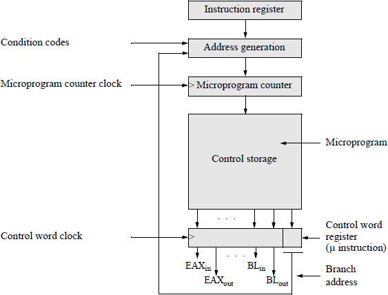
The instruction register contains the current instruction. The address generation block is set to the starting address of the microprogram for a particular instruction and is a function of the contents of the instruction register, the condition codes, and the branch address of the current control word (microinstruction). The microprogram counter is similar to the program counter (PC) of a computer — it points to the address of the next instruction. The microprogram counter is incremented by 1 or set to the branch address. The control storage block is a PROM that contains the microprogram (or firmware).
The control word register contains the current microinstruction to control the machine's hardware for a specific macroinstruction. Microinstructions are fetched from control storage in a similar manner to instructions fetched from main memory. A microinstruction has two main parts: a control field and an address field. The control field issues control lines, such as EAXin, which loads the EAX register with data at the next active clock transition; and EAXout, which gates the contents of EAX to the destination bus. The address field (branch address) indicates the address of the next microinstruction in the microprogram if a branch is required.
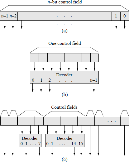
It is desirable to keep the control word as short as possible to minimize the hardware and yet have as many unique individual bits as possible to obtain high-speed execution of the macro instructions. Microinstructions (control words) are generally classifies as a horizontal format, a vertical format, or a combination format, which is a combination of vertical and horizontal formats.
The horizontal format has no decoding; therefore, it has very long formats. This provides high operating speeds with a high degree of parallelism. An example of the horizontal format is shown in Figure 2.5(a). The vertical format has a large amount of decoding; therefore, it has short formats. It operates at a slower speed due to the inclusion of a decoder and is not highly parallel. An example of the vertical format is shown in Figure 2.5(b). Most microprogrammed computers use a combination of horizontal and vertical formats. An example of the combination format is shown in Figure 2.5(c). Note that decoder output 0 cannot be used, because the field being decoded may be all zeroes.
2.4 Memory Unit
The memory unit consists primarily of main memory and cache. It also contains two registers: memory address register and memory data register. The memory address register (MAR) contains the memory address to which data are written of from which data are read. The memory data register (MDR) contains the data that is written to memory or read from memory.
2.4.1 Main Memory
The main memory, also called random access memory (RAM), contains the instructions and data for the computer. There are typically two types RAM: static RAM and dynamic RAM. Static RAM is designed using flip-flops that store one bit of information. A static RAM does not need refreshing and operates at a higher speed than dynamic RAM, but requires more hardware. Dynamic RAM stores one bit of information in a capacitor and associated hardware. Since the charge in the capacitor leaks and diminishes with time, the charge must be refreshed periodically in order to maintain the state of the data. The density of a dynamic RAM is much greater than the density of a static RAM, but operates at a slower speed.
2.4.2 Hamming Code
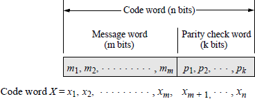
Errors can occur in the transmission or storage of information being sent to or from memory. A typical error detection and correction scheme is one developed by Richard W. Hamming. The basic Hamming code can detect single or double errors and can correct single errors. The information sent to memory is coded in the form shown in Figure 2.6. A code word contains n bits consisting of m message bits plus k parity check bits. The m bits represent the information or message part of the code word; the k bits are used for detecting and correcting errors, where .
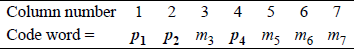
Since there can be an error in any bit position, including the parity check bits, there must be a sufficient number of k parity check bits to identify any of the m + k bit positions. The parity check bits are normally embedded in the code word and are positioned in columns with column numbers that are a power of two, as shown in Figure 2.7 for a code word containing four message bits (m3, m5, m6, m7) and three parity bits (p1, p2, p4).
Each parity bit maintains odd parity over a unique group of bits as shown in Figure 2.8 for a code word of four message bits, where E1, E2, and E4 represent the four groups.
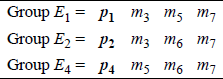
The placement of the parity bits in certain columns is not arbitrary. Each of the variables in group E1 contain a 1 in column 1 (20) of the binary representation of the column number as shown in Figure 2.9. Since p1 has only a single 1 in the binary representation of column 1, p1 can therefore be used as a parity check bit for a message bit in any column in which the binary representation of the column number has a 1 in column 1 (20). Thus, group E1 can be expanded to include other message bits, as shown below.
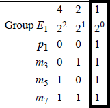
Each of the variables in group E2 contain a 1 in column 2 (21) of the binary representation of the column number as shown in Figure 2.10. Since p2 has only a single 1 in the binary representation of column 2, p2 can therefore be used as a parity check bit for a message bit in any column in which the binary representation of the column number has a 1 in column 2 (21). Thus, group E2 can be expanded to include other message bits, as shown below.
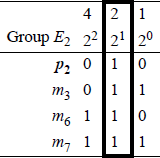
Each of the variables in group E4 contain a 1 in column 4 (22) of the binary representation of the column number as shown in Figure 2.11. Since p4 has only a single 1 in the binary representation of column 4, p4 can therefore be used as a parity check bit for a message bit in any column in which the binary representation of the column number has a 1 in column 4 (22). Thus, group E4 can be expanded to include other message bits, as shown below.
The format for embedding parity bits in the code word can be extended easily to any size message. For example, the code word for an 8-bit message is encoded as shown below, where m3, m5, m6, m7, m9, m10, m11, m12 are the message bits and p1, p2, p4, p8 are the parity check bits for groups E1, E2, E4, E8, respectively, as shown in Figure 2.12.
For messages, the bit with the highest numbered subscript is the low-order bit. Thus, the low-order message bit is m12 for a byte of data that is encoded using the Hamming code. A 32-bit message requires six parity check bits:
There is only one parity bit in each group. The parity bits are independent and no parity bit checks any other parity bit. Consider the following code word for a 4-bit message:
The parity bits are generated so that there are an odd number of 1s in the following groups: group E1, group E2, and group E4. For example, the parity bits are generated by the exclusive-NOR function as follows:
Example 2.1 A 4-bit message (0110) will be encoded using the Hamming code then transmitted. The message, transmitted code word, and received code word are shown in Figure 2.13.
From the received code word, it is apparent that bit 6 is in error. When the code word is received, the parity of each group is checked using the bits assigned to that group, as shown in Figure 2.14. A parity error is assigned a value of 1; no parity error is assigned a value of 0. The groups are then listed according to their binary weight. The resulting binary number is called the syndrome word and indicates the bit in error; in this case, bit 6, as shown in Figure 2.15. The bit in error is then complemented to yield a correct message of 0110.
Since there are three groups in this example, there are eight combinations. Each combination indicates the column of the bit in error, including the parity bits. A syndrome word of indicates no error in the received code word.
Double error detection and single error correction can be achieved by adding a parity bit for the entire code word. The format is shown below, where pcw is the parity bit for the code word.
2.4.3 Cache Memory
The memory block also includes cache memory. Cache memory is used to increase the speed of instruction execution by storing frequently-used information in the form of instructions or data. Each location in cache is referred to as a cache line. A cache is a content-addressable memory (CAM), because the memory is addressed by contents contained in memory, not by the physical address of the contents. Caches are also referred to as associative memory.
There are typically three types of cache memories that are used in current microprocessors: level 1 cache (L1), level 2 cache (L2), and level 3 (L3) cache. The L1 cache, implemented with static RAM, has high-speed access and is the primary cache. It is located on the CPU chip and is used for temporary storage of instructions and data. There are usually two L1 caches: one to store instructions and one to store data.
The L2 cache typically has a larger capacity than the L1 cache but is slower and is logically positioned between the L1 cache and main memory. In many cases, the L2 cache is also located on the CPU chip. The L2 cache is referred to as the secondary cache and is implemented with static RAM. The L2 cache is used to prefetch instructions and data for the processor, thus reducing access time.
The L3 cache is an optional cache and, if used, is usually located on the circuit board logically positioned between the L2 cache and main memory. If the system does have L1, L2, and L3 caches, then the information transfer path is from main memory to L3 to L2 to L1 to CPU.
Figure 2.16 shows the organization of memory priority in relation to the CPU. The highest speed memory is located within the CPU in the form of registers. Next is the cache subsystem (L1, L2, and L3 caches) with slower speeds than the CPU, followed by the relatively low-speed memory but with a much larger capacity. The lowest-speed memory devices are the peripheral I/O units; for example a disk subsystem with the highest capacity.
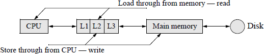
If the addressed information is not in cache during a read operation from main memory, then a block transfer is performed from main memory to cache. Execution can be increased if the addressed word is passed on to the CPU as soon as it is received from main memory. This is referred to as a load through. A store through is performed when cache and main memory are updated simultaneously.
When information is transferred from main memory to cache, there are normally three mapping algorithms that can be applied: direct mapping, associative mapping — also referred to as fully associative, and set-associative mapping — also referred to as block-set-associative. When a block is loaded from main memory into cache, a tag associated with the main memory location is assigned to the block in cache.
Direct mapping Direct mapping is the most straightforward. Assume that cache has 128 blocks and that there are 4096 blocks in main memory partitioned into 128 blocks per partition. Then block k of main memory maps into block k modulo-128 of the cache. That is, block 0, block 128, block 256, etc. all map into block 0 of cache. In a similar manner, block 1, block 129, block 257, etc. all map into block 1 of cache.
Associative mapping Associative mapping allows any block in main memory to be loaded into any cache location. This necessitates a large associative cache memory, because any cache location may contain the required information. This mapping technique yields a very high hit ratio for an associative search. The hit ratio is the percentage of cache accesses that result in a cache hit. A cache hit means that the information is in cache; a cache miss means that the information is in main memory or I/O memory.
Set-associative mapping Set-associative mapping combines the advantages of both direct and associative mapping. Blocks — or cache lines — in cache are partitioned into sets. The algorithm assigns a block in main memory to be mapped into any block of a specific set. The cache contains S sets in which each set contains L lines. Let M be the number of lines in cache. Then the set associativity of cache is L = M/S = set size. A 4-way (L = 4) set-associative cache with 1024 lines (M = 1024) has S = M/L = 256 sets. This mapping technique requires an additional field in the memory address: a set field. The algorithm first determines which set might contain the desired cache block. Then the tag field in the memory address is compared with the tags in the cache blocks of that set. The technique is direct mapping to set i; however, this is predominantly set-associative mapping, because any memory block to some modulus can map to any line in set i.
Tag field This section describes a general approach for tag comparison to determine if the requested block of data is in cache. Each cache line has a tag field associated with the data in the cache line, as shown in Figure 2.17.
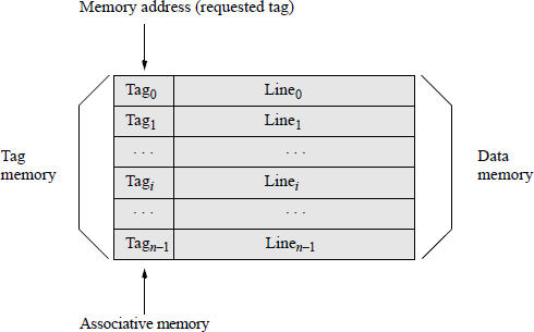
The main memory address consists of three main fields, the tag field, the block field, and the word field which selects the word in the cache. The tag field is usually the high-order bits of the main memory address and connects to the tag memory inputs of a content-addressable memory; thus, data can be identified for retrieval by the contents of the tag field rather than by the address of the data. All tags fields are compared in parallel. If the tag field in cache matches the tag field in the memory address, then a cache hit occurs and the data in that cache line is sent to the CPU. If there is no tag match, then a cache miss occurs and main memory is searched for the required block of data.
Tag fields are used in all three types of mapping: direct mapping, associative mapping, and set-associative mapping. Tag comparison is simply the exclusive-NOR of the tag field bits in the main memory address with the tag field bits in cache. This is the equality function, which generates a logic 1 if the two tags are equal.
There are also two additional bits associated with a cache line: a valid bit and a dirty bit. These bits are usually part of the tag field. The valid bit indicates whether a specific cache line contains valid data. When the system is initialized, the valid bit is set to 0. When a cache line is loaded from main memory, the valid bit is set to 1. The dirty bit (or modified bit) indicates that the cache line has been updated.
Replacement algorithms There are replacement algorithms associated with cache. When a new block is to be mapped into a cache that is full, an existing block must be replaced. For direct mapping, there is only one choice: block k of main memory maps into block k to some modulus of cache and replaces the cache block. For associative and set-associative caches, a different replacement algorithm is used.
One commonly used technique is the least-recently used (LRU) algorithm. This method replaces the block in the set which has been in the cache the longest without being referenced. For a two-block set-associative cache, in which there are two blocks per set, each of the two blocks in the set contain a USE bit. When a block is referenced, the USE bit for that block is set to 1; the USE bit for the second block is set to 0. When a block is read from main memory to be stored in cache, the cache block whose USE bit equals 0 is replaced.
For a four-block set-associative cache, containing four blocks per set, a 2-bit counter is used to determine which block in the set is least recently used. There are three conditions that determine which block is replaced depending on a cache hit or a cache miss and whether the cache is full or not full. The three conditions are shown below.
- If there is a cache hit on seti blockj, then the following operations take place:
- If blockk counter < blockj counter, then increment blockk counter.
- If blockk counter ≥ blockj counter, then do not increment blockk counter.
- Set blockj counter = 0.
- If there is a cache miss and the set is not full, then the following operations take place:
- Memory block is stored in seti blockj (empty block).
- Set blockj counter = 0.
- Increment all other counters.
- If there is a cache miss and the set is full, then the following operations take place:
- If blockj counter = 3, then remove blockj.
- Memory block is stored in seti blockj (empty block).
- Set blockj counter = 0.
- Increment all other counters.
Another replacement algorithm is called first-in, first-out. This technique replaces the block in the set which has been in the cache the longest and is implemented with a circular buffer technique, as shown below.
Tag |
Data |
|||
|---|---|---|---|---|
Block 1 |
Load block 1 first |
Remove block 1 first |
||
Seti |
Block 2 |
Load block 2 second |
Remove block 2 second |
|
Block 3 |
Load block 3 third |
Remove block 3 third |
||
Block 4 |
Load block 4 fourth |
Remove block 4 fourth |
A fourth replacement algorithm is called random replacement. A block is randomly chosen to be replaced. This is a very effective method and is only slightly inferior to the other algorithms.
2.5 Input/Output
The input/output (I/0) block of Figure 2.1 incorporates I/O peripheral devices and associated control units. Some examples of I/O device subsystems are tape, disk, keyboard, monitors, plotters, compact disks, and devices attached to a computer by means of a universal serial bus (USB). Many computers also incorporate I/O processors — called channels — to control all data and command transfers between the computer (or memory) and the I/O device. The channels are integrated into the CPU or are standalone units.
2.5.1 Tape Drives
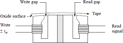
Tape drives A tape drive is sequential access storage device (SASD) and is a low-cost means of obtaining large storage. The disadvantage is that it has long access times, because it reads or writes data sequentially; that is, it cannot go directly to a record on tape, but must progress through previous records to obtain the desired record, depending on the location of the read/write heads. Figure 2.18 shows a typical tape drive head with one write head and one read head per track. Most tape subsystems utilize a read-after-write (also called read-while-write) procedure to verify that the data were written correctly.
The number of tracks per tape varies depending on the format used for the data. There are single-track drives, drives with nine tracks (one byte plus parity) for the Extended Binary-Coded Decimal Interchange Code (EBCDIC) for legacy systems, and drives with seven tracks (including parity) for BCD formats. Most current personal computer (PC) drives use the seven-track American Standard Code for Information Interchange (ASCII) format (0 through 127 decimal), which can be extended to include the remaining codes (128 through 255 decimal).
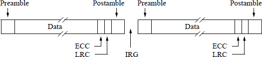
Data stored on tape can be in a variety of formats, depending on the manufacturer. A typical format is shown in Figure 2.19. The preamble is a unique combination of 1s and 0s, which are used to synchronize detection circuits to distinguish 1s from 0s. The postamble serves two purposes: It signals the end of data; and it serves as a preamble which permits a read backward operation — the functions of the preamble and postamble are then reversed. The error correcting code (ECC) is used to detect and correct errors in the data stream. The longitudinal redundancy check (LRC) is a form of horizontal redundancy check that is applied to each track. The interrecord gap (IRG) pov-ides a space for starting and stopping the tape. It allows sufficient time to decelerate and accelerate the tape between records.
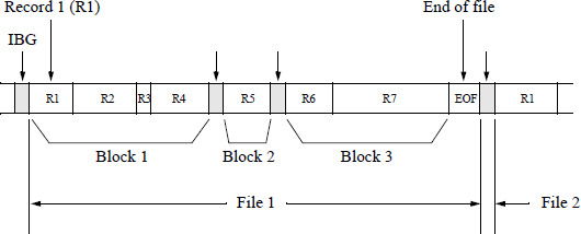
A tape with many small records requires a large number of IRGs. This decreases the efficiently of tape utilization. This inefficiency can be reduced by grouping the records into blocks with no IRGs between records. The IRGs are placed between the blocks and are called interblock gaps (IBGs). A block and file format is shown in Figure 2.20. There is only one preamble and postamble per block. An end of file gap is used to separate files. This is usually blank tape followed by a tape mark (7F hexadecimal).
2.5.2 Disk Drives
Current disk drives have a mean time between failures (MTBF) of approximately 40 years. The data rate can be calculated using Equation 2.1. The circumference as a function of the radius is required in order to obtain the data rate in bits per second. The radius changes with each track; however, the density also changes if the method of writing is fixed data transfer rate with varying linear density. As the radius increases toward the outer tracks. the density decreases. Thus, the data rate remains constant.
The read/write head is not in contact with the surface of the disk. The linear density depends on the amount of separation between the head and the disk — higher density requires closer separation. To achieve close separation, the head is flown on an air bearing and is referred to as the flying height. The bearing is simply a cushion of air that is dragged along by the rotating surface. The disk and head in current disk drives are usually contained in a sealed head-disk assembly (HDA).
Since the read/write head is expensive, there is usually only one head and one gap per surface. Therefore, it is not possible to read while writing to verify that the data were written correctly, as in tape drives. There are numerous track formats, depending on the manufacturer. One format is shown in Figure 2.21, which contains two fields for each fixed-length sector: the address field and the data field.
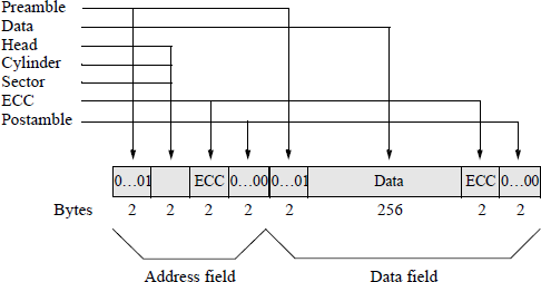
The preamble for both the address and the data field consists of two bytes — fifteen 0s followed by a single 1 — that are used for clock synchronization and to differentiate between 1s and 0s. The second two-byte segment of the address field contains the address of the cylinder, head, and sector. This is followed by two bytes containing an error correcting code (ECC). A common error correcting code is a cyclic redundancy check (CRC) code. Cyclic redundancy check codes can detect both single-bit errors and multiple-bit errors and are especially useful for large strings of serial binary data found on single-track storage devices, such as disk drives. They are also used in serial data transmission networks and in 9-track magnetic tape systems, where each track is treated as a serial bit stream.
The postamble consists of sixteen 0s and is used to separate the address and data fields. It is possible to verify a sector address then read or write the data in that sector by switching from read mode to write mode between the address and data fields.
The areal density (bits/in2) can be increased by using thin film heads which are manufactured using semiconductor technology. This technology can double the areal density and has a flying height of less than one-half the wavelength of red light — approximately 0.000075 centimeters.
2.6 Register Set
Many of the X86 microprocessors use a superscalar architecture that executes more than one instruction per clock cycle in a parallel implementation. A superscalar processor has multiple parallel pipelines in which each pipeline processes instructions from a separate instruction thread. Superscalar processors are different from multi-core processors which process multiple threads from multiple cores, one thread per core. Superscalar processors are also different than pipelined processors, which operate on multiple instructions in various stages of execution.
There are a variety of X86 processors from Intel Corporation, Advanced Micro Devices (AMD), and many other microprocessor companies. Intel processors range from the Pentium family to the dual-core and quad-core processors that support 32-and 64-bit architectures. Figure 2.22 shows a typical X86 processor register set used for most common applications in the IA-32 processor basic execution environment. There are other registers that are not shown, such as those used for memory management; single-instruction multiple-data (SIMD); packed floating-point operations; control registers; debug registers; machine check registers; and the 64-bit registers with R prefix, among others.
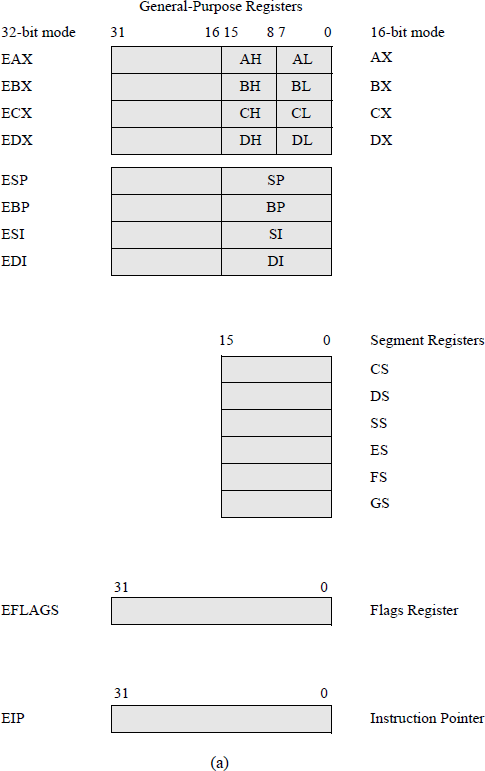
Typical X86 register set for most common applications in the IA-32 basic execution environment: (a) general-purpose registers and (b) floating-point registers.
2.6.1 General-Purpose Registers
The eight general-purpose registers (GPRs) can be addressed separately as 8-bit registers, as 16-bit registers, or as 32-bit registers, such as AL, AX, or EAX, for example. Register AL specifies the low-order eight bits of register AX; register AH specifies the high-order eight bits of register AX; register AX specifies the low-order 16 bits of register EAX. The general-purpose registers are used for arithmetic operations, logical operations, and for addressing memory.
Although they are referred to as general-purpose registers, each register has a specific application. Register EAX and its constituent registers are used as the accumulator; specifically, as the dividend for unsigned and signed divide operations, as the multiplicand for unsigned and signed multiply operations, and for input/output operations. Register AL is also used for the translate (XLAT) instruction.
Register EBX and its constituent registers are used as index registers for base addressing and as pointers to data in the data segment (DS). The effective address (EA) is the sum of a displacement value and the contents of one of the EBX registers. When these registers are used, the default location of the operand resides in the current data segment.
The ECX register and its constituent registers are the implied counters for certain instructions; for example, to count the number of iterations in a loop. The CL register is also used to indicate the shift amount when shifting or rotating bits left or right. For string operations, the ECX register set denotes the number of operands that are moved from the source string to the destination string.
The EDX register and its associated registers — generally referred to as the data registers — are used for input/output operations and for multiply and divide operations for both unsigned and signed operands. The multiplicand (destination operand — AL, AX, or EAX) is multiplied by the multiplier (source operand in a GPR or memory) and the product is stored in the destination operand. The product is stored in register AX, concatenated register pair DX:AX, or concatenated register pair EDX:EAX, depending on the size of the 2n-bit result. The destination operand in 64-bit mode is RDX:RAX. For a divide operation, the 2n-bit dividend in registers AX, DX:AX, EDX:EAX, or RDX:RAX is divided by the n-bit divisor (source operand in a GPR or memory). The resulting quotient is stored in AL, AX, EAX, or RAX. The remainder is stored in register AH, DX, EDX, or RDX.
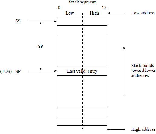
Register SP (for 16-bit stack words) or register ESP (for 32-bit stack double-words) are stack pointers that point to the current top of stack by providing an offset from the stack segment register address to point to the last valid entry in the stack. Figure 2.23 shows a stack of 16-bit words using SP as the stack pointer. When a word is pushed onto the stack in this figure, SP is first decremented by two, then the word is stored on the stack. SP points to the new top of stack (TOS) containing the last valid entry. When a word is popped off the stack, the word is first stored in the destination, then SP is incremented by two.
The BP and EBP registers are base pointers that are used to point to data on the stack; for example, parameters pushed onto the stack by one program to be accessed by another program via the stack. The base pointer registers provide an offset from the stack segment register address to point to the required data.
The SI and ESI registers are source index registers that are used for string operations. They provide an offset in the data segment (DS) that points to the beginning of a source string that is to be transferred to a destination string in the extra segment (ES).
The DI and EDI registers are destination index registers that are used for string operations. They provide an offset in the extra segment that points to the beginning address of a destination string that is to be transferred from a source string in the data segment.
2.6.2 Segment Registers
When using a segmented memory model in the IA-32 processors, memory is partitioned into independent segments for code, data, and stack. The code segment (CS) register — segment selector — contains the starting address of the computer's code segment. The offset in the instruction pointer (IP or EIP) points to a particular instruction in the code segment. The combination of the segment selector and the offset is the logical address of the next instruction to be executed.
There are four data segments: DS, ES, FS, and GS. The data segment (DS) register contains the starting address of the program's data segment. This address plus the offset value indicates the logical address of the required data. The contents of the extra segment (ES) register plus an offset in the destination index (DI) register points to a destination address in the extra segment for string operations. The FS and GS registers are available for different data structures.
2.6.3 EFLAGS Register
The 32-bit EFLAGS register is partitioned into three groups of flags: status flags, control flags, and system flags, as shown in Figure 2.24.
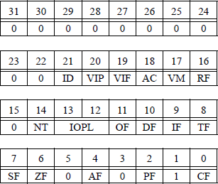
Status flags The carry flag (CF) is set if there is a carry out of or a borrow into the high-order bit position of an arithmetic operation; otherwise it is reset. It is also used with shift and rotate instructions.
The parity flag (PF) is set if the low-order byte of the result has an even number of 1s; otherwise it is reset. The adjust flag (AF or auxiliary carry) is set if there is a carry out of or a borrow into the low-order four bits — used primarily for a binary-coded decimal arithmetic operation; otherwise it is reset. The zero flag (ZF) is set if the result is zero; otherwise it is reset. The sign flag (SF) is set to the value of the high-order bit position, which is the sign bit for signed operands. If the sign flag is 0, then the result is positive; if the sign flag is 1, then the result is negative.
The overflow flag (OF) is set if the result of an operation is too large or too small to be contained in the destination operand; that is, the number is out of range for the size of the result. An interrupt-on-overflow (INTO) instruction generates an interrupt if the overflow flag is set. The equations to detect overflow for two n-bit operands A and B are shown in Equation 2.2, where an–1 and bn–1 are the sign bits of A and B, respectively and sn–1 is the sign of the result. The carry bits out of positions n–1 and n–2 are cn–1 and cn–2, respectively.
Control flag The direction flag (DF) indicates the direction for string operations and is used for the following string instructions: move string (MOVS), compare strings (CMPS), scan string (SCAS), load string (LODS), and store string (STOS). If the direction flag is reset, then this causes the string instruction to auto-increment the index registers (SI and DI); that is, to process strings from left (low address) to right (high address). If the direction flag is set, then this causes the string instruction to auto-decrement the index registers (SI and DI); that is, to process strings from right (high address) to left (low address).
System flags The system flags are used to control the operating system and CPU operations. For example, if the interrupt enable flag (IF) is set and an interrupt occurs, then this causes the CPU to transfer control to a memory location specified by an interrupt vector. The CPU can temporarily ignore maskable interrupts, but must respond immediately to non-maskasble interrupts, such as non-recoverable hardware errors, time-critical interrupts, or power failure. If the interrupt enable flag is reset, then interrupts are disabled.
The trap flag (TF) allows single-step mode for debugging; that is, single instruction execution. The CPU generates an interrupt after each instruction so that the program and results can be examined.
The nested task (NT) flag is set if the present task is nested within another task. The two bits of the input/output privilege level (IOPL) flag contain the I/O privilege level of the current task and supports multitasking. An IOPL of 00 is the highest level; an IOPL of 11 is the lowest level. The privilege levels are used with the privileged instructions, such as input/output instructions and segment accessibility.
The resume flag (RF), when set, indicates to the CPU to resume debugging. The debug software sets the flag prior to returning to the interrupted program. When the virtual-8086 mode (VM) flag is set, the CPU emulates the program environment of the 8086 processor; when reset, the processor returns to protected mode. Protected mode permits the CPU to use virtual memory, paging, and multi-tasking features.
The alignment check (AC) flag is used to check the alignment of memory references. It is set if a word (16 bits) or doubleword (32 bits) is not on a word or doubleword boundary. The virtual interrupt flag (VIF) is a virtual image of the interrupt flag and is used in combination with the virtual interrupt pending (VIP) flag. The VIP flag is set if an interrupt is pending and reset if there is no interrupt pending.
If a program has the capability to set or reset the identification (ID) flag, then the processor supports the CPU identification (CPUID) instruction. The CPUID instruction returns the processor identification in certain general registers.
2.6.4 Instruction Pointer
The instruction pointer (EIP) contains the offset for the current code segment that points to the next instruction to be executed. The EIP is updated as shown below for sequential execution, where (EIP) specifies the ‘contents of’ EIP. The EIP register is used for 32-bit mode; the RIP register is used for 64-bit mode.
The EIP progresses from one instruction to the next in sequential order, or forwards/backwards a specified number of instructions for jump (JMP), jump on condition (Jcc), return from a procedure/subroutine (RET), or return from interrupt (IRET) instructions.
2.6.5 Floating-Point Registers
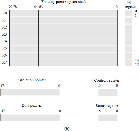
The floating-point unit (math coprocessor) provides a high-performance floatingpoint processing component for use with the IEEE Standard 754. It provides support for floating-point, integer, and binary-coded decimal operands for use in engineering and other applications. The floating-point registers were shown in Figure 2.22(b).
Data registers There are eight 80-bit data registers, R0 through R7, whose functions are similar to that a stack. Any Ri can be assigned as top of stack (T0S). Data are stored in these registers in the double extended-precision floating-point format consisting of a sign bit (79), a 15-bit exponent field (78 through 64), and a 64-bit signif-icand/fraction (63 through 0). The implied 1 is to the immediate left of bit position 63, but is not shown. Data that are loaded into the floating-point data registers are converted to the double extended-precision floating-point format.
There are no push and pop instructions the floating-point register stack. A load (push) operation is accomplished decreasing the stack top by 1, then loading the operand into the new top of stack (T0S). This is similar to a regular stack which builds toward lower addresses. A store (pop) operation is accomplished by storing the operand from the current stack top to the destination, then increasing stack top by 1. If a load is to be executed when the stack top is R0, then the registers wrap around making the new stack top R7. This may generate an overflow condition if the contents of R7 were not previously saved.
Tag register The 16-bit tag register specifies the condition of the individual data registers. There are two bits per register that are defined as shown in Figure 2.25. A tag of 10 indicates a special floating-point number, such as not-a-number (NaN), a value of infinity, a denormal number, or unsupported format.
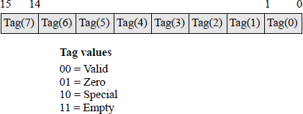
A denormal number has a biased exponent of zero. NaN is a value that does not depict a numeric or infinite quantity. It is a value that is generally produced as the result of an arithmetic operation using invalid operands. For example, calculating the square root of a negative number. NaNs can also be used to represent missing values in arithmetic calculations.
Status register The format for the 16-bit status word register is shown in Figure 2.26. The status word indicates the condition of the floating-point unit. It can be inspected by first storing the status word into a memory location and then transferring it to a general register. If a bit is set, then this indicates an active condition.
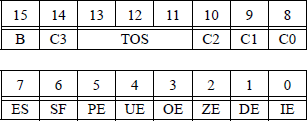
Bit 15 indicates that the floating-point unit is busy (B). The condition code bits C3 through C0 are specified by bits 14, 10, 9, and 8, respectively. They represent the result of certain floating-point arithmetic operations. The condition code is used primarily for conditional branching. Bits 13 through 11 indicate the top of stack (TOS) pointer, as shown below.
Bits |
||||
|---|---|---|---|---|
13 |
12 |
11 |
Stack top |
|
0 |
0 |
0 |
= |
Register 0 |
0 |
0 |
1 |
= |
Register 1 |
0 |
1 |
0 |
= |
Register 2 |
0 |
1 |
1 |
= |
Register 3 |
1 |
0 |
0 |
= |
Register 4 |
1 |
0 |
1 |
= |
Register 5 |
1 |
1 |
0 |
= |
Register 6 |
1 |
1 |
1 |
= |
Register 7 |
Bit 7 is the exception summary status (ES) bit, which is set if any of the unmasked exception flags — bits 5 through 0 — in the status word are set. The exception flags in the status word can be prevented from being set by setting the corresponding exception mask bit in the control word register.
Bit 6 is the stack fault (SF) bit, which is set if a stack overflow or stack underflow has been detected. Bit 5 is the precision exception (PE) bit, which is set if the result of an operation cannot be precisely represented in the destination format. Bit 4 is the underflow exception (UE) bit, which is set whenever the rounded normalized result of an arithmetic operation is too small to be contained in the destination operand. Bit 3 is the overflow exception (OE) bit, which is set whenever the rounded normalized result of an arithmetic operation is too large to be contained in the destination operand. Bit 2 is the divide-by-zero exception (ZE) bit, which is set whenever an instruction attempts to divide an operand by zero, where the dividend is a nonzero operand.
Bit 1 is the denormalized operand exception (DE) bit. If the biased exponent of a floating-point number is zero, then extremely small numbers can be represented by setting the high-order bits of the fraction (significand) to zero, thus allowing very small numbers to be realized. Numbers in this range are referred to as denormalized numbers. A number that is denormalized may result in a loss of precision. If the exponent is zero and the significand is also zero, then this is usually specified as a value of zero. Therefore, a number is denormalized if the exponent is zero and the fraction is not all zeroes. Denormalized numbers are located around the value of zero.
Bit 0 is the invalid operation exception (IE), which is set whenever there is a stack overflow, a stack underflow, or when an invalid arithmetic operand has been detected. When the stack fault bit is set in the status word register, the invalid operation was caused by a stack overflow or underflow. When the stack fault bit is reset in the status word register, the invalid operation was caused by an invalid operand.
Control register The format for the control word register is shown in Figure 2.27. The control word provides several processing options by loading a word from memory into the 16-bit control word register. Blank entries in the register are reserved. The control word register manages the precision, rounding methods, and masking. The control word register is initialized to the following states: round to nearest, 64-bit double extended precision, and set the six exception mask flags to one.
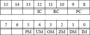
Bit 12 is the infinity control (IC) bit, which is used to allow compatibility with older versions of floating-point units. Bit 11 and bit 10 are the rounding control field bits that determine the rounding method used in arithmetic operations. The four different types of rounding techniques are shown in Table 2.1 and explained in the paragraphs that follow.
Rounding Control Field
Rounding Method |
11 |
10 |
|---|---|---|
Round to nearest (default mode) |
0 |
0 |
Round down toward minus infinity |
0 |
1 |
Round up toward positive infinity |
1 |
0 |
Round toward zero (truncate) |
1 |
1 |
The round to nearest mode is the default rounding method, which provides the nearest approximation to the result. The result of a floating-point arithmetic operation can be rounded to the nearest number that contains n bits. This method is also called adder-based rounding and rounds the result to the nearest approximation that contains n bits. The operation is as follows: The bits to be deleted are truncated and a 1 is added to the retained bits if the high-order bit of the deleted bits is a 1. When a 1 is added to the retained bits, the carry is propagated to the higher-order bits. If the addition results in a carry out of the high-order bit position, then the fraction is shifted right one bit position and the exponent is incremented.
Consider the fraction 0.b–1 b–2 b–3 b–4 1 x x x — where the xs are 0s or 1s — which is to be rounded to four bits. Using the adder-based rounding technique, this rounds to 0.b–1 b–2 b–3 b–4 + 0.0001. The retained bits of fraction 0.b–1 b–2 b–3 b–4 0 x x x round to 0.b–1 b–2 b–3 b–4. The first fraction approaches the true value from above; the second fraction approaches the true value from below. Examples of adder-based rounding are shown in Figure 2.28 and illustrate approaching the true value from above and approaching the true value from below.
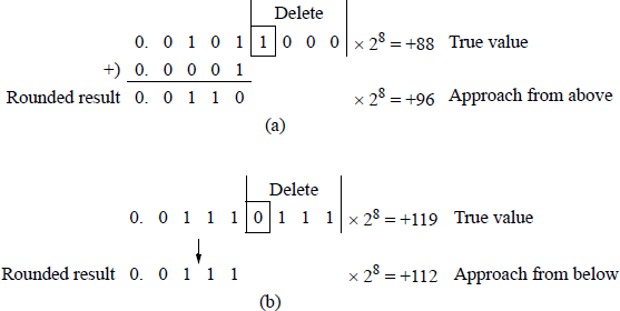
Adder-based rounding: (a) true value approached from above and (b) true value approached from below.
The rounding mode of round down toward minus infinity (also referred to as directed rounding) produces a solution that is nearest to but no greater than the result. This technique rounds towards negative infinity. It stipulates that the result of an arithmetic operation should be the value closest to negative infinity; that is, a value that is algebraically less than the precise result.
The rounding mode of round up toward positive infinity (also referred to as directed rounding) produces a solution that is nearest to but no less than the result. This technique rounds towards positive infinity. It stipulates that the result of an arithmetic operation should be the value closest to positive infinity; that is, a value that is algebraically greater than the precise result.
The rounding mode of round toward zero is also referred to as truncation or chopping. Truncation deletes extra bits and makes no changes to the retained bits. This makes the truncated value less than or equal to the original value. Aligning fractions during addition or subtraction could result is losing several low-order bits, so there is obviously an error associated with truncation. Assume that the following fraction is to be truncated to four bits:
Then all fractions in the range 0.b–1 b–2 b–3 b–4 0000 to 0.b–1 b–2 b–3 b–4 1111 will be truncated to 0.b–1 b–2 b–3 b–4. The error ranges from 0 to .00001111. In general, the error ranges from 0 to approximately 1 in the low-order position of the retained bits. Truncation is a fast and easy method for deleting bits resulting from a fraction underflow and requires no additional hardware. Fraction underflow can occur when aligning fractions during addition or subtraction when one of the fractions is shifted to the right. There is one disadvantage in that a significant error may result.
There is another method of rounding called von Neumann rounding. The von Neumann rounding method is also referred to as jamming and is similar to truncation. If the bits to be deleted are all zeroes, then the bits are truncated and there is no change to the retained bits. However, if the bits to be deleted are not all zeroes, then the bits are deleted and the low-order bit of the retained bits is set to 1.
Thus, when 8-bit fractions are rounded to four bits, fractions in the range
will all be rounded to 0.b–1 b–2 b–3 1. Therefore, the error ranges from approximately –1 to +1 in the low-order bit of the retained bits when
and when
Although the error range is larger in von Neumann rounding than with truncation rounding, the error range is symmetrical about the ideal rounding line and is an unbiased approximation. Assuming that individual errors are evenly distributed over the error range, then positive errors will be inclined to offset negative errors for long sequences of floating-point calculations involving rounding. The von Neumann rounding method has the same total bias as adder-based rounding; however, it requires no more time than truncation.
Bit 9 and bit 8 represent the precision control field and set the precision at 64 bits, 53 bits, or 24 bits, as defined in Table 2.2. The default precision is double extended precision using a 64-bit significand — bit 63 through bit 0 — thereby providing a high degree of precision.
Precision Control Field
Precision |
9 |
8 |
|---|---|---|
Single precision (24 bits) |
0 |
0 |
Reserved |
0 |
1 |
Double precision (53 bits) |
1 |
0 |
Double extended precision (64 bits) |
1 |
1 |
Bit 5 through bit 0 are designated as exception mask bits for certain exceptions; if a bit is set, then the exception is masked. The exception mask bits in the control word register correspond directly to the exception flag bits in the same position in the status word register. When a mask bit is set, the corresponding exception is blocked from being produced.
Instruction pointer and data pointer The instruction and data pointer registers contain pointers to the instruction and data for the last non-control instruction executed; if a control instruction is executed, then the register contents remain unchanged for both the instruction pointer and the data pointer. The data register contains a pointer for a memory operand. These pointers are stored in 48-bit registers — a segment selector is stored in bit 47 through bit 32; a memory offset is stored in bit 31 through bit 0.
2.7 Translation Lookaside Buffer
Another common component that is inherent in the architecture of current microprocessors is a translation lookaside buffer (TLB). A TLB is a cache used by the memory management unit to increase the speed of virtual-to-physical address translation. A TLB is generally a content-addressable memory in which each virtual (or logical) address is a tag in cache that is associated with a physical address. Since the TLB is an associative memory, comparison of the virtual address with the corresponding tags is accomplished in parallel. If the desired virtual address is in cache, then this is a TLB hit and the physical address thus obtained is used to address main memory.
TLBs contain instruction addresses and data addresses of the most recently used pages. A page is a fixed-length area of memory that consists of blocks of contiguous memory locations. The virtual address is formed by a virtual page number and an offset — the high-order and low-order bits, respectively. The virtual address is applied to the TLB and to the system cache concurrently. If the address is not in main memory, then the contents are retrieved from a direct-access storage device and stored in main memory; this is referred to as page-in technique. When transferring a page in main memory to an external storage device, this is referred to as a page-out technique. At any given time, main memory contains only a portion of the total contents of virtual memory.
There are advantages in utilizing a virtual memory technique: More efficient use of main memory is achieved; only the amount of main memory that is needed at the time is used; that is, programs are not present in memory if they are not being used; an application program can be designed that exceeds the main memory size, thus a program's address space is not bound by the amount of main (real) memory. When a program does not fit completely into memory, the parts that are not currently being executed are stored in secondary storage, such as a disk subsystem.
The relative (virtual) address of an instruction or operand is translated into a real (physical) address only when the virtual address is referenced. This type of translation is called dynamic relocation and is executed by a hardware component called dynamic address translation. Address translation occurs whenever an instruction or operand is referenced (addressed) during program execution.
2.8 The Assembler
There are various levels of programming in a computer. The lowest level is machine level programming in which the program is entered using a binary, octal, or hexadecimal number system. This is a tedious method and is prone to errors. The next higher level is assembly language programming in which the program is entered using symbolic instructions, such as MOV, ADD, SAR, etc., which represent a move instruction, an add instruction, and a shift arithmetic right instruction, respectively. Assembly language programming is machine dependent and requires an assembler, which translates the instructions into the required bit pattern of 1s and 0s.
The next popular higher level language currently in use is C programming, which is machine independent; that is, unlike an assembly language, it can be run on any computer with little or no alteration. C programs require a compiler to generate machine code. Other languages in this category are Fortran, PL1, Basic, and Pascal, among others. The next higher level language is the popular C++ programming language, which is classified as an object-oriented programming language and maintains the integrity and support for C. Another object-oriented programming language is Java, which is used for general-purpose programming and World Wide Web programming.
An interpreter translates a single instruction, written in a high-level language, to machine code before executing the instruction. A compiler translates all instructions in the source code program to machine (object) code before executing the program. A compiler translates source code from a high-level language to a low-level language, such as assembly language and may generate many lines of machine code. An assembler translates one line of source code to one line of machine code.
2.8.1 The Assembly Process
There are many different versions of an X86 assembler, such as Microsoft Assembler (MASM), Turbo Assembler (TASM), Flat Assembler (FASM), and Netwide Assembler (NASM), among others. The X86 assembler translates an assembly language program into a relocatable object file that can be linked with other object files to generate an executable file.
An editor is used to create an assembler source program which is saved as a .asm file. Then the assembler translates the source program to machine code and generates an object program .obj. For example, if the source code was to move an immediate operand of 0123H to register AX, then the source code would be MOV AX, 23 01. This translates to the following hexadecimal machine code: B8 23 01.
The next task is to link the .obj program and create an executable program .exe. Because a program can be loaded anywhere in memory, the assembler may not have generated all the addresses. Also, there may be other programs to link. Therefore, the link program
(1) Completes address generation.
(2) Combines more than one assembled module into an executable program.
(3) Initializes the .exe module for loading the program for execution.
For a simple two-pass assembler, the following steps take place during each pass:
Pass 1: |
(1) The assembler reads the entire symbolic program. |
(2) The assembler makes a symbol table of names and labels; for example, data field labels. |
|
(3) The assembler determines the amount of code to be generated. |
|
Pass 2: |
(1) The assembler now knows the length and relative position of each data field and instruction. |
(2) The assembler can now generate the object code with relative addresses. |
2.9 Problems
- 2.1 Three code words, each containing a message of four bits which are encoded using the Hamming code, are received as shown below. Determine the correct 4-bit messages that were transmitted using odd parity.
Received Code Words |
|||||||
|---|---|---|---|---|---|---|---|
Bit Position |
1 |
2 |
3 |
4 |
5 |
6 |
7 |
(a) |
0 |
1 |
0 |
1 |
0 |
1 |
0 |
(b) |
1 |
1 |
0 |
0 |
1 |
1 |
0 |
(c) |
0 |
0 |
1 |
0 |
1 |
1 |
1 |
2.2 An 11-bit message is to be encoded using the Hamming code with odd parity. Write the equations for all of the groups that are required for the encoding process.
2.3 The 7-bit code words shown below are received using Hamming code with odd parity. Determine the syndrome word for each received code word.
(a)
(b)
- 2.4 A code word containing one 8-bit message, which is encoded using the Hamming code with odd parity, is received as shown below. Determine the 8-bit message that was transmitted.
Bit Position |
1 |
2 |
3 |
4 |
5 |
6 |
7 |
8 |
9 |
10 |
11 |
12 |
Received Code Word |
0 |
1 |
0 |
1 |
1 |
0 |
0 |
1 |
0 |
0 |
1 |
1 |
- 2.5 A code word containing one 8-bit message, which is encoded using the Hamming code with odd parity, is received as shown below. Determine the 8-bit message that was transmitted.
Bit Position |
1 |
2 |
3 |
4 |
5 |
6 |
7 |
8 |
9 |
10 |
11 |
12 |
Received Code Word |
1 |
1 |
0 |
0 |
1 |
0 |
1 |
1 |
0 |
0 |
0 |
1 |
- 2.6 A code word containing one 12-bit message, which is encoded using the Hamming code with odd parity, is received as shown below. Determine the syndrome word.
1 |
2 |
3 |
4 |
5 |
6 |
7 |
8 |
9 |
10 |
11 |
12 |
13 |
14 |
15 |
16 |
17 |
1 |
0 |
1 |
1 |
1 |
1 |
1 |
0 |
0 |
0 |
1 |
0 |
1 |
1 |
1 |
0 |
1 |
2.7 Obtain the code word using the Hamming code with odd parity for the following message word: 1 1 0 1 0 1 0 1 1 1 1.
2.8 Determine the relative merits of horizontal and vertical microinstruction formats.
2.9 Discuss the advantages and disadvantages of hardwired and microprogrammed control.
2.10 A block-set-associative cache consists of a total of 64 blocks (lines) divided into four-block sets. Determine the number of sets in cache.
2.11 Perform the arithmetic operations shown below with fixed-point binary numbers in 2s complement representation. In each case, indicate if there is an overflow.
(a)
(b)
(c)
2.12 Let A and B be two binary integers in 2s complement representation as shown below, where A′ and B′ are the diminished radix complement of A and B, respectively. Determine the result of the operation and indicate if an overflow exists.
- 2.13 A fraction and the bits to be deleted (low-order three bits) are shown below. Determine the rounded results using truncation (round toward zero), adder-based rounding (round to nearest), and von Neumann rounding.
Fraction |
|||||||||||
|---|---|---|---|---|---|---|---|---|---|---|---|
. |
0 |
0 |
1 |
0 |
1 |
0 |
0 |
1 |
1 |
0 |
1 |
2.14 Let the augend be
Let the addend be
Perform the addition operation and round the result using all three rounding methods.
2.15 Let the augend be
Let the addend be
Perform the addition operation and round the result using all three rounding methods.