This chapter is going to give you a general understanding of the fundamentals of computer functioning. We will describe a core model of computation, enumerate its extensions, and take a closer look at two of them, namely, registers and hardware stack. It will prepare you to start assembly programming in the next chapter.
1.1 The Core Architecture
1.1.1 Model of Computation
What does a programmer do? A first guess would probably be “construction of algorithms and their implementation.” So, we grasp an idea, then we code, and this is the common way of thinking.
Can we construct an algorithm to describe some daily routine, like going out for a walk or shopping? The question does not sound particularly hard, and many people will gladly provide you with their solutions.
However, all these solutions will be fundamentally different. One will operate with such actions as “opening the door” or “taking the key”; the other will rather “leave the house,” omitting details. The third one, however, will go rogue and provide a detailed description of the movement of his hands and legs, or even describe his muscle contraction patterns.
The reason those answers are so different is the incompleteness of the initial question.
All ideas (including algorithms) need a way to be expressed. To describe a new notion we use other, simpler notions. We also want to avoid vicious cycles, so the explanation will follow the shape of a pyramid. Each level of explanation will grow horizontally. We cannot build this pyramid infinitely, because the explanation has to be finite, so we stop at the level of basic, primitive notions, which we have deliberately chosen not to expand further. So, choosing the basics is a fundamental requirement to express anything.
It means that algorithm construction is impossible unless we have fixed a set of basic actions, which act as its building blocks.
Model of computation is a set of basic operations and their respective costs.
The costs are usually integer numbers and are used to reason about the algorithms’ complexity via calculating the combined cost of all their operations. We are not going to discuss computational complexity in this book.
Most models of computation are also abstract machines. It means that they describe a hypothetical computer, whose instructions correspond to the model’s basic operations. The other type of models, decision trees, is beyond the scope of this book.
1.1.2 von Neumann Architecture
Now let us imagine we are living in 1930s, when today’s computers did not yet exist. People wanted to automate calculations somehow, and different researchers were coming up with different ways to achieve such automation. Common examples are Church’s Lambda calculus or the Turing machine. These are typical abstract machines, describing imaginary computers.
One type of machine soon became dominant: the von Neumann architecture computer.
Computer architecture describes the functionality, organization, and implementation of computer systems. It is a relatively high-level description, compared to a calculation model, which does not omit even a slight detail.
von Neumann architecture had two crucial advantages : it was robust (in a world where electronic components were highly unstable and short-lived) and easy to program.
In short, this is a computer consisting of one processor and one memory bank, connected to a common bus. A central processing unit (CPU) can execute instructions, fetched from memory by a control unit. The arithmetic logic unit (ALU) performs the needed computations. The memory also stores data. See Figures 1-1 and 1-2.
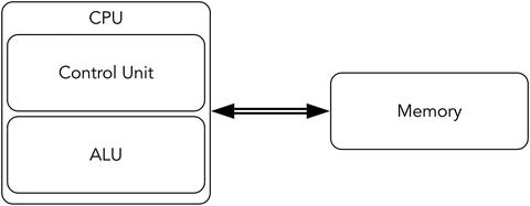
Figure 1-1. von Neumann architecture—Overview
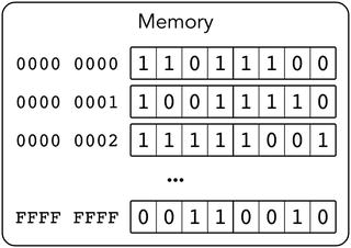
Figure 1-2. von Neumann architecture—Memory
Following are the key features of this architecture:
Memory stores only bits (a unit of information, a value equal to 0 or 1).
Memory stores both encoded instructions and data to operate on. There are no means to distinguish data from code: both are in fact bit strings.
Memory is organized into cells, which are labeled with their respective indices in a natural way (e.g., cell #43 follows cell #42). The indices start at 0. Cell size may vary (John von Neumann thought that each bit should have its address); modern computers take one byte (eight bits) as a memory cell size. So, the 0-th byte holds the first eight bits of the memory, etc.
The program consists of instructions that are fetched one after another. Their execution is sequential unless a special jump instruction is executed.
Assembly language for a chosen processor is a programming language consisting of mnemonics for each possible binary encoded instruction (machine code). It makes programming in machine codes much easier, because the programmer then does not have to memorize the binary encoding of instructions, only their names and parameters.
Note, that instructions can have parameters of different sizes and formats.
An architecture does not always define a precise instruction set, unlike a model of computation.
A common modern personal computer have evolved from old von Neumann architecture computers, so we are going to investigate this evolution and see what distinguishes a modern computer from the simple schematic in Figure 1-2.
Note
Memory state and values of registers fully describe the CPU state (from a programmer’s point of view). Understanding an instruction means understanding its effects on memory and registers.
1.2 Evolution
1.2.1 Drawbacks of von Neumann Architecture
The simple architecture described previously has serious drawbacks .
First of all, this architecture is not interactive at all. A programmer is limited by manual memory editing and visualizing its contents somehow. In the early days of computers, it was pretty straightforward, because the circuits were big and bits could have been flipped literally with bare hands.
Moreover, this architecture is not multitask friendly. Imagine your computer is performing a very slow task (e.g., controlling a printer). It is slow because a printer is much slower than the slowest CPU. The CPU then has to wait for a device reaction a percentage of time close to 99%, which is a waste of resources (namely, CPU time).
Then, when everyone can execute any kind of instruction, all sorts of unexpected behavior can occur. The purpose of an operating system (OS) is (among others) to manage the resources (such as external devices) so that user applications will not cause chaos by interacting with the same devices concurrently. Because of this we would like to prohibit all user applications from executing some instructions related to input/output or system management.
Another problem is that memory and CPU performance differ drastically.
Back in the old times, computers were not only simpler: they were designed as integral entities. Memory, bus, network interfaces—everything was created by the same engineering team. Every part was specialized to be used in this specific model. So parts were not destined to be interchangeable. In these circumstances none tried to create a part capable of higher performance than other parts, because it could not possibly increase overall computer performance.
But as the architectures became more or less stable, hardware developers started to work on different parts of computers independently. Naturally, they tried to improve their performance for marketing purposes. However, not all parts were easy and cheap 1 to speed up. This is the reason CPUs soon became much faster than memory . It is possible to speed up memory by choosing other types of underlying circuits, but it would be much more expensive [12].
When a system consists of different parts and their performance characteristics differ a lot, the slowest part can become a bottleneck. It means that if is the slowest part is replaced with a faster analogue, the overall performance will increase significantly. That’s where the architecture had to be heavily modified.
1.2.2 Intel 64 Architecture
In this book we only describe the Intel 64 architecture .2
Intel has been developing its main processor family since the 1970s. Each model was intended to preserve the binary compatibility with older models. It means that even modern processors can execute code written and compiled for older models. It leads to a tremendous amount of legacy. Processors can operate in a number of modes: real mode, protected, virtual, etc. If not specified explicitly, we will describe how a CPU operates in the newest, so-called long mode.
1.2.3 Architecture Extensions
Intel 64 incorporates multiple extensions of von Neumann’s architecture. The most important ones are listed here for a quick overview.
Registers These are memory cells placed directly on the CPU chip. Circuit-wise they are much faster, but they are also more complicated and expensive. Register accesses do not use the bus. The response time is quite small and usually equals a couple of CPU cycles. See section 1.3 “Registers”.
Hardware stack A stack in general is a data structure. It supports two operations: pushing an element on top of it and popping the topmost element. A hardware stack implements this abstraction on top of memory through special instructions and a register, pointing at the last stack element. A stack is used not only in computations but to store local variables and implement function call sequence in programming languages. See section 1.5 “Hardware stack”.
Interrupts This feature allows one to change program execution order based on events external to the program itself. After a signal (external or internal) is caught, a program’s execution is suspended, some registers are saved, and the CPU starts executing a special routine to handle the situation. Following are exemplary situations when an interrupt occurs (and an appropriate piece of code is executed to handle it):
A signal from an external device.
Zero division.
Invalid instruction (when CPU failed to recognize an instruction by its binary representation).
An attempt to execute a privileged instruction in a non-privileged mode. See section 6.2 “Interrupts” for a more detailed description.
Protection rings A CPU is always in a state corresponding to one of the so-called protection rings. Each ring defines a set of allowed instructions. The zero-th ring allows executing any instruction from the entire CPU’s instruction set, and thus it is the most privileged. The third allows only the safest ones. An attempt to execute a privileged instruction results in an interrupt. Most applications are working inside the third ring to ensure that they do not modify crucial system data structures (such as page tables) and do not work with external devices, bypassing the OS. The other two rings (first and second) are intermediate, and modern operating systems are not using them.
See section 3.2 “Protected mode” for a more detailed description.
Virtual memory This is an abstraction over physical memory, which helps distribute it between programs in a safer and more effective way. It also isolates programs from one another.
See section 4.2 “Motivation” for a more detailed description.
Some extensions are not directly accessible by a programmer (e.g., caches or shadow registers). We will mention some of them as well.
Table 1-1 summarizes information about some von Neumann architecture extensions seen in modern computers.
Table 1-1. von Neumann Architecture: Modern Extensions
Problem | Solution |
|---|---|
Nothing is possible without querying slow memory | Registers, caches |
Lack of interactivity | Interrupts |
No support for code isolation in procedures, or for context saving | Hardware stack |
Multitasking: any program can execute any instruction | Protection rings |
Multitasking: programs are not isolated from one another | Virtual memory |
Sources of information
No book should cover the instruction set and processor architecture completely. Many books try to include exhaustive information about instruction set. It gets outdated quite soon; moreover, it bloats the book unnecessarily.
We will often refer you to Intel® 64 and IA-32 Architectures Software Developer’s Manual available online: see [15]. Get it now!
There is no virtue in copying the instruction descriptions from the “original” place they appear in; it is much more mature to learn to work with the source.
The second volume covers instruction set completely and has a very useful table of contents. Please, always use it to get information about instruction set: it is not only a very good practice, but also a quite reliable source.
Note, that many educational resources devoted to assembly language in the Internet are often heavily outdated (as few people program in assembly these days) and do not cover the 64-bit mode at all. The instructions present in older modes often have their updated counterparts in long mode, and those are working in a different way. This is a reason we strongly discourage using search engines to find instruction descriptions, as tempting as it might be.
1.3 Registers
The data exchange between CPU and memory is a crucial part of computations in a von Neumann computer. Instructions have to be fetched from memory, operands have to be fetched from memory; some instructions store results also in memory. It creates a bottleneck and leads to wasted CPU time when it waits for the data response from the memory chip. To avoid constant wait, a processor was equipped with its own memory cells, called registers. These are few but fast. Programs are usually written in such a way that most of the time the working set of memory cells is small enough. This fact suggests that programs can be written so that most of the time the CPU will be working with registers.
Registers are based on transistors, while main memory uses condensers. We could have implemented main memory on transistors and gotten a much faster circuit. There are several reasons engineers prefer other ways of speeding up computations .
Registers are more expensive.
Instructions encode the register’s number as part of their codes. To address more registers the instructions have to grow in size.
Registers add complexity to the circuits to address them. More complex circuits are harder to speed up. It is not easy to set up a large register file to work on 5 GHz.
Naturally, register usage slows down computers in the worst case. If everything has to be fetched into registers before the computations are made and flushed into memory after, where’s the profit?
The programs are usually written in such a way, that they have one particular property. It is a result of using common programming patterns such as loops, function, and data reusage, not some law of nature. This property is called locality of reference and there are two main types of it: temporal and spatial.
Temporal locality means that accesses to one address are likely to be close in time.
Spatial locality means that after accessing an address X the next memory access will likely to be close to X, (like X − 16 or X + 28).
These properties are not binary: you can write a program exhibiting stronger or weaker locality.
Typical programs are using the following pattern: the data working set is small and can be kept inside registers. After fetching the data into registers once we will work with them for quite some time, and then the results will be flushed into memory. The data stored in memory will rarely be used by the program. In case we need to work with this data we will lose performance because
We need to fetch data into the registers.
If all registers are occupied with data we still need later on, we will have to spill some of them, which means save their contents into temporally allocated memory cells.
Note
A widespread situation for an engineer: decreasing performance in the worst case to improve it in average case. It does work quite often, but it is prohibited when building real-time systems, which impose constraints on the worst system reaction time. Such systems are required to issue a reaction to events in no more than a certain amount of time, so decreasing performance in the worst case to improve it in other cases is not an option.
1.3.1 General Purpose Registers
Most of the time, programmer works with general purpose registers. They are interchangeable and can be used in many different commands.
These are 64-bit registers with the names r0, r1, …, r15. The first eight of them can be named alternatively; these names represent the meaning they bear for some special instructions. For example, r1 is alternatively named rcx, where c stands for “cycle.” There is an instruction loop, which uses rcx as a cycle counter but accepts no operands explicitly. Of course, such kind of special register meaning is reflected in documentation for corresponding commands (e.g., as a counter for loop instruction). Table 1-2 lists all of them; see also Figure 1-3.
Table 1-2. 64-bit General Purpose Registers
Name | Alias | Description |
|---|---|---|
r0 | rax | Kind of an “accumulator,” used in arithmetic instructions. For example, an instruction div is used to divide two integers. It accepts one operand and uses rax implicitly as the second one. After executing div rcx a big 128-bit wide number, stored in parts in two registers rdx and rax is divided by rcx and the result is stored again in rax. |
r3 | rbx | Base register. Was used for base addressing in early processor models. |
r1 | rcx | Used for cycles (e.g., in loop). |
r2 | rdx | Stores data during input/output operations. |
r4 | rsp | Stores the address of the topmost element in the hardware stack. See section 1.5 “Hardware stack”. |
r5 | rbp | Stack frame’s base. See section 14.1.2 “Calling convention”. |
r6 | rsi | Source index in string manipulation commands (such as movsd) |
r7 | rdi | Destination index in string manipulation commands (such as movsd) |
r8 | ||
r9 … r15 | no | Appeared later. Used mostly to store temporal variables (but sometimes used implicitly, like r10, which saves the CPU flags when syscall instruction is executed. See Chapter 6 “Interrupts and system calls”). |
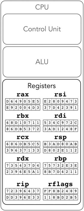
Figure 1-3. Approximation of Intel 64: general purpose registers
Note
Unlike the hardware stack, which is implemented on top of the main memory, registers are a completely different kind of memory. Thus they do not have addresses, as the main memory’s cells do!
The alternate names are in fact more common for historical reasons. We will provide both for reference and give a tip for each one. These semantic descriptions are given for a reference; you don’t have to memorize them right now.
You usually do not want to use rsp and rbp registers because of their very special meaning (later we will see how they corrupt stack and stack frame). However, you can perform arithmetic operations on them directly, which makes them general purpose.
Table 1-3 shows registers sorted by their names following an indexing convention.
Table 1-3. 64-Bit General Purpose Registers—Different Naming Conventions
r0 | r1 | r2 | r3 | r4 | r5 | r6 | r7 |
rax | rcx | rdx | rbx | rsp | rbp | rsi | rdi |
Addressing a part of a register is possible. For each register you can address its lowest 32 bits, lowest 16 bits, or lowest 8 bits.
When using the names r0,...,r15 it is done by adding an appropriate suffix to a register’s name:
d for double word—lower 32 bits;
w for word—lower 16 bits;
b for byte—lower 8 bits.
For example,
r7b is the lowest byte of register r7;
r3w consists of the lowest two bytes of r3; and
r0d consists of the lowest four bytes of r0.
The alternate names also allow addressing the smaller parts.
Figure 1-4 shows decomposition of wide general purpose registers into smaller ones.
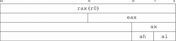
Figure 1-4. rax decomposition
The naming convention for accessing parts of rax, rbx, rcx, and rdx follows the same pattern; only the middle letter (a for rax) is changing. The other four registers do not allow an access to their second lowest bytes (like rax does by the name of ah). The lowest byte naming differs slightly for rsi, rdi, rsp, and rbp.
The smallest parts of rsi and rdi are sil and dil (see Figure 1-5).
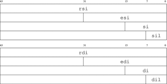
Figure 1-5. rsi and rdi decomposition
The smallest parts pf rsp and rbp are spl and bpl (see Figure 1-6).
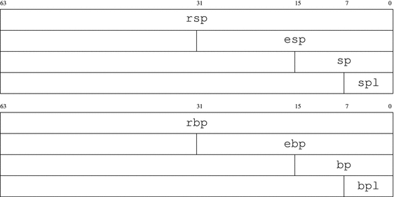
Figure 1-6. rsp and rbp decomposition
In practice, the names r0- r7 are rarely seen. Usually programmers stick with alternate names for the first eight general purpose registers. It is done for both legacy and semantic reasons: rsp relates a lot more information, than r4. The other eight (r8-r15) can only be named using an indexed convention.
Inconsistency in writes
All reads from smaller registers act in an obvious way. The writes into 32-bit parts, however, fill the upper 32 bits of the full register with sign bits. For example, zeroing eax will zero the entire rax, storing -1 into eax will fill the upper 32 bits with ones. Other writes (e.g., in 16-bit parts) act as intended: they leave all other bits unaffected. See section 3.4.2 “CISC and RISC” for the explanation.
1.3.2 Other Registers
The other registers have special meaning. Some registers have system-wide importance and thus cannot be modified except by the OS.
A programmer has access to rip register . It is a 64-bit register, which always stores an address of the next instruction to be executed. Branching instructions (e.g., jmp) are in fact modifying it. So, every time any instruction is being executed, rip stores the address of the next instruction to be executed.
Note
All instructions have different size!
Another accessible register is called rflags. It stores flags, which reflect the current program state—for example, what was the result of the last arithmetic instruction: was it negative, did an overflow happened, etc. Its smaller parts are called eflags (32 bit) and flags (16 bit).
Question 1
It is time to do preliminary research based on the documentation [15]. Refer to section 3.4.3 of the first volume to learn about register rflags. What is the meaning of flags CF, AF, ZF, OF, SF? What is the difference between OF and CF?
In addition to these core registers there are also registers used by instructions working with floating point numbers or special parallelized instructions able to perform similar actions on multiple pairs of operands at the same time. These instructions are often used for multimedia purposes (they help speed up multimedia decoding algorithms). The corresponding registers are 128-bit wide and named xmm0 - xmm15. We will talk about them later.
Some registers have appeared as non-standard extensions but became standardized shortly after. These are so-called model-specific registers . See section 6.3.1 “Model specific registers” for more details.
1.3.3 System Registers
Some registers are designed specifically to be used by the OS. They do not hold values used in computations. Instead, they store information required by system-wide data structures. Thus their role is supporting a framework, born from a symbiosis of the OS and CPU. All applications are running inside this framework. The latter ensures that applications are well isolated from the system itself and from one another; it also manages resources in a way more or less transparent for a programmer.
It is extremely important that these registers are inaccessible by applications themselves (at least the applications should not be able to modify them). This is the goal of privileged mode (see section 3.2).
We will list some of these registers here. Their meaning will be explained in detail later.
cr0, cr4 store flags related to different processor modes and virtual memory;
cr2, cr3 are used to support virtual memory (see sections 4.2 “Motivation”, 4.7.1 “Virtual address structure”);
cr8 (aliased as tpr) is used to perform a fine tuning of the interrupts mechanism (see section 6.2 “Interrupts”).
efer is another flag register used to control processor modes and extensions (e.g., long mode and system calls handling).
idtr stores the address of the interrupt descriptors table (see section 6.2 “Interrupts”).
gdtr and ldtr store the addresses of the descriptor tables (see section 3.2 “Protected mode”).
cs, ds, ss, es, gs, fs are so-called segment registers. The segmentation mechanism they provide is considered legacy for many years now, but a part of it is still used to implement privileged mode. See section 3.2 “Protected mode”.
1.4 Protection Rings
Protection rings are one of the mechanisms designed to limit the applications’ capabilities for security and robustness reasons. They were invented for Multics OS, a direct predecessor of Unix. Each ring corresponds to a certain privilege level. Each instruction type is linked with one or more privilege levels and is not executable on others. The current privilege level is stored somehow (e.g., inside a special register).
Intel 64 has four privilege levels, of which only two are used in practice: ring-0 (the most privileged) and ring-3 (the least privileged). The middle rings were planned to be used for drivers and OS services, but popular OSs did not adopt this approach.
In long mode, the current protection ring number is stored in the lowest two bits of register cs (and duplicated in those of ss). It can only be changed when handling an interrupt or a system call. So an application cannot execute an arbitrary code with elevated privilege levels: it can only call an interrupt handler or perform a system call. See Chapter 3 “Legacy” for more information.
1.5 Hardware Stack
If we are talking about data structures in general, a stack is a data structure, a container with two operations: a new element can be placed on top of the stack (push); the top element can be taken away from the stack (pop).
There is a hardware support for such data structure. It does not mean there is also a separate stack memory. It is just sort of an emulation implemented with two machine instructions (push and pop) and a register (rsp). The rsp register holds an address of the topmost element of the stack. The instructions perform as follows:
push argument
Depending on argument size (2, 4, and 8 bytes are allowed), the rsp value is decreased by 2, 4, or 8.
An argument is stored in memory starting at the address, taken from the modified rsp.
pop argument
The topmost stack element is copied into the register/memory.
rsp is increased by the size of its argument. An augmented architecture is represented in Figure 1-7.
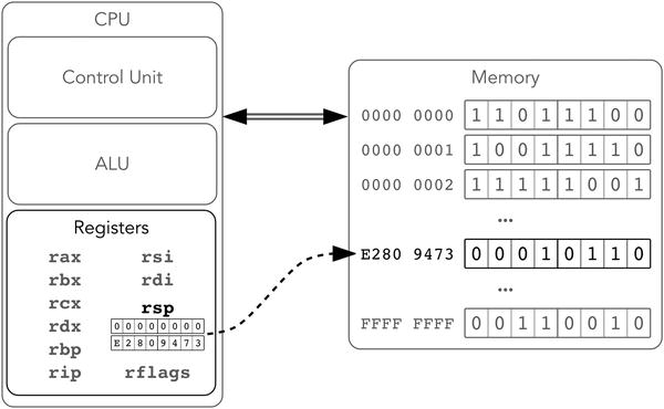
Figure 1-7. Intel 64, registers and stack
The hardware stack is most useful to implement function calls in higher-level languages. When a function A calls another function B, it uses the stack to save the context of computations to return to it after B terminates.
Here are some important facts about the hardware stack, most of which follow from its description:
There is no such situation as an empty stack, even if we performed push zero times. A pop algorithm can be executed anyway, probably returning a garbage “topmost” stack element.
Stack grows toward zero address.
Almost all kinds of its operands are considered signed integers and thus can be expanded with sign bit. For example, performing push with an argument B916 will result in the following data unit being stored on the stack:
0xff b9, 0xffffffb9 or 0xff ff ff ff ff ff ff b9.By default, push uses an 8-byte operand size. Thus an instruction push -1 will store 0xff ff ff ff ff ff ff ff on the stack.
Most architectures that support stack use the same principle with its top defined by some register. What differs, however, is the meaning of the respective address. On some architectures it is the address of the next element, which will be written on the next push. On others it is the address of the last element already pushed into the stack.
Working with Intel docs: How to read instruction descriptions
Open the second volume of [15]. Find the page corresponding to the push instruction. It begins with a table. For our purpose we will only investigate the columns OPCODE, INSTRUCTION, 64-BIT MODE, and DESCRIPTION. The OPCODE field defines the machine encoding of an instruction (operation code). As you see, there are options and each option corresponds to a different DESCRIPTION. It means that sometimes not only the operands vary but also the operation codes themselves.
INSTRUCTION describes the instruction mnemonics and allowed operand types. Here R stands for any general purpose register, M stands for memory location, IMM stands for immediate value (e.g., integer constant like 42 or 1337). A number defines operand size. If only specific registers are allowed, they are named. For example:
push r/m16—push a general purpose 16-bit register or a 16-bit number taken from memory into the stack.
push CS—push a segment register cs.
The DESCRIPTION column gives a brief explanation of the instruction’s effects. It is often enough to understand and use the instruction.
Read the further explanation of push. When is the operand not sign extended?
Explain all effects of the instruction push rsp on memory and registers.
1.6 Summary
In this chapter we provided a quick overview of von Neumann architecture. We have started adding features to this model to make it more adequate for describing modern processors. So far we took a closer look at registers and the hardware stack. The next step is to start programming in assembly, and that is what the next chapter is dedicated to. We are going to view some sample programs, pinpoint several new architectural features (such as endianness and addressing modes), and design a simple input/output library for *nix to ease interaction with a user.
Question 2
What are the key principles of von Neumann architecture?
Question 3
What are registers?
Question 4
What is the hardware stack?
Question 5
What are the interrupts?
Question 6
What are the main problems that the modern extensions of the von Neumann model are trying to solve?
Question 7
What are the main general purpose registers of Intel 64?
Question 8
What is the purpose of the stack pointer?
Question 9
Can the stack be empty?
Question 10
Can we count elements in a stack?