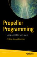
One of the main uses of a Propeller is to “talk” to hardware such as motors, relays, switches, LEDs, and so on. In the Propeller there are 32 general-purpose input/output pins, P0–P31. Figure 7-1 shows an overview of the relationship between the cogs and pins. Pins P30 and P31 are usually reserved for the programming and serial ports. Pins P28 and P29 are usually tied to an electrically erasable programmable read-only memory (EEPROM) that stores the program even when there is no power applied. So, pins P0–P27 are available for general input/output use.
Again, I must emphasize that all the cogs can run in parallel, so they can interact with the pins at the same time. If a cog has declared a pin an input, then it can read the value of that pin at the same time as other cogs do. If a pin is declared an output by more than one cog, then the output of that pin is the logical OR of the output of those cogs.
Three registers control these pins.
- DIRA is a 32-bit register that controls the direction of the pin associated with each bit. If bit N of this register is 1, then the corresponding pin P<N> will be an output, and if it is zero, that pin will be an input.
- OUTA is a 32-bit register that sets the value of a pin P<N> by setting or clearing the associated bit N. These pins will be affected only if the value of the associated DIRA bit is set to output (1).
- INA is a 32-bit register that reflects the value of the signal on pin P<N>. A low voltage (0–0.7V) is a zero on the associated bit N of the register, and a high voltage (2.7–3.3V) is a 1. Again, bitN of DIRA should be set to input (0).
Figure 7-1
Block diagram of the Propeller showing the cogs and pins
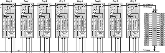
All eight cogs have access to all of the pins. Each of the cogs has its own independent DIRA, INA, and OUTA registers. The output of a pin is what is “agreed on” by all the cogs. If more than one cog declares a pin as output, then the pin will be high if any of those cogs sets it high. The pin will be low if all of those cogs set it low. In Figure 7-2, a switchman is manually operating a switch that controls which track a train will take.
A pin will be an input if no active cog has it as an output.
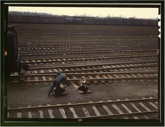
Figure 7-2
Switchman throwing a switch at the Chicago and NW Railroad Proviso yard, Chicago, IL, 1942. Photo by Jack Delano; available at the Library of Congress Farm Security Administration archives.
www.loc.gov/pictures/item/fsa1992000705/PP/
.
To view the result of setting a pin, a logic analyzer is useful. A logic analyzer
attaches to a pin and displays the logical state of the pin as a function of time (1 or 0). Unlike an oscilloscope, you can monitor multiple pins (usually 8 or 16), and importantly, the logic analyzer software is aware of common protocols such as Universal Serial Receive/Transmit (UART), Serial Peripheral Interface (SPI), Inter-Integrated Communication (I2C), and so on. (I am partial to the Logic8 from Saleae.1) See also the Papilio Logic Analyzer.2
7.1 Outline
In this chapter we will read and set the value of pins in both Spin and PASM. We will look at the SPI communication protocol (a common method for communicating between embedded devices). We will implement SPI between cogs as a way to log data from a PASM cog to the main Spin code. Finally, I introduce the concept of semaphores or locks that allow two cogs to interact without confusion or conflict. This is a dense chapter, so feel free to refer to it if and when you need it!
7.2 Timing in Spin and PASM
Instructions in Spin
run slowly compared to the same instruction in PASM (by an order of magnitude or more). In addition, in Spin, the amount of time an instruction takes to complete is subject to change. By contrast, the timing of PASM instructions is short (generally four clock cycles) and unvarying. For applications that require precise and rapid timing (high-frequency clocks or monitoring a high data rate line), PASM
is preferred. Each PASM instruction has a known number of clock cycles to complete.
1 CON ' Clock mode settings
2 _CLKMODE = XTAL1 + PLL16X
3 _XINFREQ = 5_000_000
4
5 ' system freq as a constant
6 FULL_SPEED = ((_clkmode - xtal1) >> 6) * _xinfreq
7 ' ticks in 1ms
8 ONE_MS = FULL_SPEED / 1_000
9 ' ticks in 1us
10 ONE_US = FULL_SPEED / 1_000_000
- Lines 2–3: These define the clock speed of the Propeller. _XINFREQ is the frequency of the crystal oscillator. _CLKMODE is a register that sets the CLK register to (in this case) generate a clock that is 16 times the oscillator frequency.
- Line 6: Here we define a constant for the number of clock ticks in one second. It is somewhat cryptic, but in short, XTAL1 and PLL16X are predefined constants. The expression _CLKMODE - XTAL1 = PLL16X = 0x40_00.
Therefore, PLL16X >> 6 = 16 (right shift by 6 bits). Finally, multiply that by the oscillator frequency. This is a reliable way to get the startup clock speed.
7.3 Spin
In Spin
these registers are usually set as shown in Listing 7-1.
1 CON
2 BLUE = 10 ' blue led
3
4 PUB MAIN
5 DIRA~ ' set all pins low (no output)
6 OUTA[BLUE] := 0 ' set pin 10 low
7 DIRA[BLUE] := 1 ' set pin 10 to output
8 repeat
9 ! OUTA[BLUE] ' toggle pin 10
10 PAUSE_MS(1000)
Listing 7-1
Toggle a Pin in Spin (ch7/io0.spin)
- Line 5: The tilde (~) after a variable says to set that variable to zero.
- Line 7: When the array form of addressing (arr[j]) is used with a register (DIRA[BLUE]), the effect is to address individual bits. In this case, only bit 10 of DIRA is set to 1, so P10 is set to output.
- Line 9: The exclamation mark (!) is a bitwise negation of the bit OUTA[BLUE], which will toggle pin P10.
- If we wish to read the value on a line, the Spin code is shown in Listing 7-2:
1 CON
2 SW = 11 ' normally open, high
3 SWMASK = |< SW ' set pin <SW> high
4 INPIN = 12
5
6 PUB MAIN | val
7 DIRA~ ' set all pins low (no output)
8
9 ' initially wait until switch is open (high)
10 waitpeq(SWMASK, SWMASK, 0) ' wait until high
11 repeat
12 waitpne(SWMASK, SWMASK, 0) ' wait for it to go low
13 val := INA[INPIN]
14 waitpeq(SWMASK, SWMASK, 0) ' wait for release of switch
Listing 7-2
Read a Switch and Pin (ch7/io1.spin)
- Line 3: Set bit 11 of SWMASK high. The operator |< is referred to as a “Decode” operator that sets the bit corresponding to the number in SW.
- Line 10: SWMASK is used in two ways here: waitpeq(Value , Mask , 0). The first argument to waitpeq (Value) is the value that the Propeller will compare against the values of the input pins that are set in the Mask argument. In other words, bit 11 is 1 in Value; bit 11 is 1 in Mask. Compare the value 1 to bit 11 of INA, and wait until they are equal, that is, until P11 is high.
- Line 12: Similar to waitpeq , waitpne waits until the Value argument is not equal to the pins set in Mask. Bit 11 of Value is 1, so wait until P11 is not 1.
- Line 13: To read the value of a line, simply read the value of a bit of the INA register.
7.4 PASM
In PASM
the same registers (DIRA, OUTA, and INA) are available at the addresses (unsurprisingly) dira, outa, and ina. These addresses are registers in the reserved part of the cog. Recall that when a cog is launched, 512 longs are copied to the cog RAM, of which the last 16 longs are reserved registers (including our old friend par).
7.4.1 Toggle a Pin in PASM
Similar to the Spin code in Listing 7-1, we toggle the value of a pin once a second but using PASM, as shown in Listing 7-3.
1 ...
2 ' << ADD THESE LINES
3 CON
4 BLUE = 10
5 SW = 11
6 INPIN = 12
7 ONESEC = ((_clkmode - xtal1) >> 6) * _xinfreq
8
9 VAR
10 ...
11 byte rdpinCogId ' << ADD THIS
12
13 PUB MAIN
14 ...
15 ' << ADD THESE LINES
16 rdpinCogId := cognew (@RDPIN, 0)
17 UARTS.STR(DEBUG, string (" rdpinCogId : "))
18 UARTS.DEC(DEBUG, rdpinCogId)
19 UARTS.PUTC(DEBUG, CR)
20 UARTS.PUTC(DEBUG, LF)
21
22 ' << ADD THESE LINES
23 DAT ' RDPIN
24
25 RDPIN ORG 0
26 mov dira, #0 wz ' set all pins to input
27 muxnz outa, _cblueMask ' set pin low
28 muxz dira, _cblueMask ' set led pin to output
29
30 mov r0, cnt
31 add r0, _coneSec
32 :loop
33 waitcnt r0, _coneSec
34 xor outa, _cblueMask
35 jmp #:loop
36
37 _cblueMask long |< BLUE
38 _cswMask long |<SW
39 _coneSec long ONESEC
40 r0 res 1
41 FIT 496
42
43 ' Program ends here
Listing 7-3
Toggle a Pin in PASM (ch7/io2-pasm.spin)
- Line 26: Set all pins to input. The wz effect will set Z.
- Line 27–28: Set pin BLUE (10) low before setting it to be an output. The muxnz outa, _cblueMask instruction says to set the pins in outa that are referenced in _cblueMask to the value of NOT Z (outa[_cblueMask] := !Z. In other words, pin 10 is set in _cblueMask, so set pin 10 of outa to !Z, which is 0. muxz sets dira[_cblueMask] := Z, which sets pin 10 to be an output.
- Lines 30–33: Set r0 to the current counter value plus one second worth of counts. Wait until the counter reaches that value (waitcnt will increment r0 by _coneSec when it expires so it is ready for the next waitcnt).
- Line 34: Toggle the output pin 10. xor outa, _cblueMask is the bitwise exclusive OR of the value of the output pins and the mask register (which has pin 10 set high). The result is written back to outa. So, if outa[10] == 1, then 1 XOR 1 = 0, and outa[10] is set to zero. If outa[10] == 0, then 0 XOR 1 = 1, and outa[[10] is set to one.
7.4.2 Monitor a Switch
As in Listing 7-2, we monitor a switch and then read the value of a pin when the switch closes, as shown in Listing 7-4.
1 CON
2 BLUE = 10
3 SW = 11
4 INPIN = 12
5 ONESEC = ((_clkmode - xtal1) >> 6) * _xinfreq
6
7 DAT
8 STEIM ORG 0
9
10 mov dira, #0 wz ' set all pins to input
11 waitpeq _cswMask, _cswMask
12 :loop
13 waitpne _cswMask, _cswMask
14 test _cinMask, ina wc
15 rcl _cval, #1
16 waitpeq _cswMask, _cswMask
17 jmp #:loop
18
19 _cblueMask long |< BLUE
20 _cswMask long |<SW
21 _cinMask long |< INPIN
22 _coneSec long ONESEC
23 r0 res 1
Listing 7-4
Read a Pin in PASM (ch7/io2-pasm.spin)
- Line 11: As in the Spin code, waitpeq Value, Mask waits until the pins in INA that are referenced in Mask are equal to Value.”
- Line 13: waitpne waits until Mask is not equal to the value.
- Lines 14–15: To read a pin, test _cinMask, ina wc will set C flag to the bitwise AND of the mask and the ina register. rcl _cval, #1 will move the C flag into the low bit of _cval.
7.5 Communication Protocols
There are number of common ways to send data from one device to another on a small number of lines, including UART, I2C, and the 1-Wire protocols. These are commonly classed as serial communication channels because the bits are transmitted over time. In contrast, a parallel channel would use a number of lines to send the bits at the same time. In Figure 7-3, an early serial communication device is shown: an electric telegraph which would visually display the signal transmitted from the other end.
A widely used serial protocol for interdevice communications is the SPI bus. The SPI protocol requires four lines for bidirectional communications between a so-called master and multiple slave devices. The SPI protocol
uses a bitwise data transmission mechanism, with a bit sent by both sides (and that bit received by the other side) at each SPI clock cycle. The SPI clock frequency is typically a few hundred kilohertz to a few megahertz. Here we will use an 8kHz clock.
SPI communications
are bidirectional, but one of the two ends is designated the master, and the other is the slave. The master will control the timing of the transfer by generating the select signal and the SPI clock, and the slave will read from the master.
Figure 7-3
Five-needle electric telegraph invented by Charles Wheatstone (of the Wheatstone bridge), 1837. The telegraph was used to signal when trains arrived and left stations. Now at the London Science Museum. Photo by Wikipedia user Geni; license CC-BY-SA GFDL.
The slave will also write to the master at the same time. Therefore, the master cannot set a pace that is too fast for the slave to keep up with.
SPI is fundamentally quite simple (though the devil is in the details). To send a number from master to slave, the master indicates the beginning of the transfer by pulling the select line low. It then toggles a clock and makes sure that each successive bit of the number is ready on the active edge of the clock (generally the rising edge). After the bits are all sent, the master pulls the select line high. At the other end, the slave waits until the select line is low. It then watches the clock line and receives a bit at each active edge. The end of the transfer is signaled by the select line going high.
- Select: The select or chip select (CS) line (active low) selects the slave devices with which the master wants to communicate and determines the start and end of communications. The master device generates this signal.
- Clock: The SPI clock line (SCLK) controls the timing of data transmission. The most common arrangement is for the rising edge of the clock to be the one at which data is exchanged and the falling edge is when the two sides are free to change the data on that line. The master device generates the clock.
- Data out: The data out or master out or master out/slave in (MOSI) line is where the data from the master to the slave is placed. The master device will ensure that a data bit is stable on the line prior to the rising edge of the clock. This is because on the rising edge, the slave device reads the value. The master should keep the data on this line stable until the falling edge because the slave could read it at any time between the rising and falling edges.
- Data in: The data in or master in or master in/slave out (MISO) line is where data from the slave to the master is placed. The master will read the MISO line on the rising edge of SCLK. Thus, at each rising edge of SCLK, a bit is sent from master to slave and from slave to master.
The interpretation of the bits (whether big- or little-endian, number of bits, and so on) is entirely up to agreement between the slave and the master. Figure 7-4 shows the case where we have 8 bits. The red lines are the active edges at which the MOSI line is read by the slave. The blue lines are when the master can change the value of the MOSI line in preparation for the next active edge.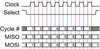
Figure 7-4
SPI timing diagram
for the case when the clock starts out low (CPOL=0) and the data is required to be valid on a rising edge (CPHA=0)
7.6 SPI Logging
The values on the pins can be set by any cog and read by any cog. That means we can use them to communicate between cogs. We will use that as a logging facility where the PASM cog will write to the SPI bus and the Spin cog will read from it. As the Spin cog is slower, it must control the transactions. In other words, the PASM cog is the master, and the Spin cog is the slave.
We are going to write an SPI logging utility. The Spin cog (main) will request a log value, and a PASM cog (logtst) will transmit the log value. The main cog will read that value and print it out. The handshaking between the cogs is as follows:
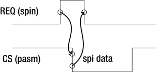
- The PASM cog will block, waiting for the REQ line to be asserted (set to the active level, in this case raised).
- When the main cog (the slave) is ready to receive a log value, it will raise the REQ line.
- This will signal the PASM cog (the master) to initiate an SPI transfer by lowering the CS line (the CS line is active low, so it is asserted by lowering it).
- The falling CS line will signal the main cog to lower the REQ line so that no further SPI transfers start until the main cog has finished with the current one and has successfully printed the value.
Figure 7-5 shows the output of a logic analyzer (LA)
. The LA
can monitor and trigger on individual lines (here I triggered on REQ on channel 0). In addition, logic analyzers can interpret well-known communication protocols such as the RS-232 serial protocol, the I2C protocol, and, as in this case, the SPI protocol. I have informed the LA of the four SPI lines, the endianness and length of the data, and the phase and polarity of the clock; the LA can interpret the data on the MOSI and MISO lines and display the result. In this example, the MOSI line is showing a 32-bit number that was transmitted MSB first and is interpreted as 0x2A.
In the Spin code (Listing 7-5), we define the pins, start the spitst cog, and assert the REQ line. When the CS line is asserted by the PASM cog, we read the log value and then re-assert the REQ line.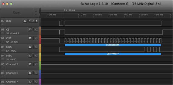
Figure 7-5
Logic analyzer display
1 ...
2 CON
3 REQ = 0
4 CS = 1
5 CLK = 2
6 MOSI = 3
7 MISO = 4
8
9 CSMASK = |<CS
10 CLKMASK = |<CLK
11 VAR
12 byte logCogId
13
14 ...
15
16 PUB MAIN | x, x0, logVal
17 ...
18 logCogId := -1
19
20 ' set the REQ line low, then set it as an output line
21 ' all others are inputs
22 outa[REQ] := 0
23 dira ~ ' all lines in
24 dira[REQ] := 1 ' req out
25
26 SPILOG.INIT
27 logCogId := SPILOG.START
28 UARTS.STR(DEBUG, string(CR, LF, " logCogId : "))
29 UARTS.DEC(DEBUG, logCogId)
30 UARTS.PUTC(DEBUG, CR)
31 UARTS.PUTC(DEBUG, LF)
32
33 ' wait here until PASM cog sets CS line high
34 waitpeq(CSMASK, CSMASK, 0)
35
36 ' OK ready for SPI
37 outa[REQ] := 1 ' assert req
38 repeat
39 ' wait for cs mask to go low
40 waitpne(CSMASK, CSMASK, 0)
41 !outa[REQ] ' lower req
42 logVal := READ_SPILOG 'read 32 bits
43 UARTS.HEX(DEBUG, logVal, 8) ' print out logVal
44 UARTS.PUTC(DEBUG, CR)
45 UARTS.PUTC(DEBUG, LF)
46 !outa[REQ] ' raise req and loop
Listing 7-5
SPI Logging, Spin Side (ch7/spi-log Demo.spin)
- Lines 3–7: Define pins .
- Lines 22–24: Set all pins to input for main cog, except for REQ.
- Lines 26–27: Launch the SPILOG PASM cog.
- Line 34: Make sure CS is high (that is, not currently in an SPI transfer). Assert REQ.
- Lines 40–46: Wait until the CS line is lowered by the PASM cog, immediately de-assert the REQ line, read a log value, and print it. Raise the REQ line to signal that the main cog is ready for another log value. Repeat.
The actual SPI read is done
with the method shown in Listing 7-6.
1 PUB READ_SPILOG : logVal | b
2 logVal := 0
3 repeat 32
4 waitpeq(CLKMASK, CLKMASK, 0)
5 b := INA[MOSI]
6 waitpne(CLKMASK, CLKMASK, 0)
7 logVal <<= 1
8 logVal |= b
Listing 7-6
Method to Read 32 Bits from SPI
The actual SPI read
is straightforward; it waits for the clock line to go high (waitpeq), reads a bit (b := INA[MOSI]), and shifts it into logVal, as follows:
1 logVal <<= 1
2 logVal |= b
- Line 1: Shift the bits in logVal left by one position.
- Line 2: b is the value read earlier (either 0 or 1). By OR-ing it with logVal, we set the lowest bit to the value of b.
The waitpne instruction is there so that we wait until the clock line goes low before looping so that we don’t read the same bit twice.
7.6.1 PASM SPI Write
The core of the PASM SPI write
is shown in Listing 7-7 and the code following the listing, with two subroutines that set the pins and do the actual writing.
1 DAT 'spilog
2 SPILOG ORG 0
3
4 call #SETUP_PINS
5
6 mov _clogVal, #42
7 call #WRITE_SPI
8 ...
Listing 7-7
SPI Logging, PASM Side (ch7/spi-log.spin)
- Line 4: Set up the REQ pin as input and the SPI pins as outputs.
- Lines 6–7: Place the log value to be transmitted into _clogVal and call WRITE_SPI to transmit. WRITE_SPI will wait for REQ to be raised and will then transmit _clogVal on the SPI lines.
The subroutine to set the pins (SETUP_PINS) is shown in Listing 7-8.
1 SETUP_PINS
2 mov dira, #0, wz
3
4 muxz outa, _ccsMask 'preset cs high, and then to output
5 muxz dira, _ccsMask
6 muxnz outa, _cclkMask ' preset clk low
7 muxz dira, _cclkMask
8 muxnz outa, _cmosiMask ' preset mosi low
9 muxz dira, _cmosiMask
10 SETUP_PINS_ret ret
Listing 7-8
Subroutine to set the SPI pins’ direction
- Line 2: Set all pins to inputs.
- Lines 4–5: Set CS high and then set CS to output.
- Lines 6–9: Set CLK and MOSI low and then set them to output.
In Listing 7-9, we do the actual work of writing 32 bits to the MOSI line. First we wait for the REQ line to be asserted, then we loop 32 times, setting the MOSI line appropriately (with a short wait between bits).
1 WRITE_SPI
2 waitpeq _creqMask, _creqMask
3 mov r0, #32 wz ' Z is set = 0
4 mov _cdt, cnt
5 add _cdt, _cEighthMS
6 waitcnt _cdt, _cEighthMS
7
8 ' lower cs
9 xor outa, _ccsMask
10
11 ' tx 32 bits, msb first
12 :spiloop
13 rol _clogVal, #1 wc ' set C from high bit of logVal
14 muxc outa, _cmosiMask ' set mosi to C
15
16 muxnz outa, _cclkMask ' raise clock (Z=0 from above)
17 waitcnt _cdt, _cEighthMS
18 xor outa, _cclkMask ' lower clock
19 waitcnt _cdt, _cEighthMS
20 djnz r0, #:spiloop
21
22 ' raise cs
23 xor outa, _ccsMask
24 WRITE_SPI_ret ret
25 ...
26 _cdt long 0
27 _cOneSec long ONE_SEC
28 _cOneMS long ONE_MS
29 _cOneUS long ONE_US
30 _cEighthMS long ONE_MS >> 3
31
32 _creqMask long |<REQ
33 _ccsMask long |<CS
34 _cclkMask long |<CLK
35 _cmosiMask long |< MOSI
Listing 7-9
Subroutine to transmit the data on MOSI
- Line 13: Set the loop index and set Z to zero.
- Lines 14–16: Set_cdt to the current counter, add 1/8ms (125us), and wait until then. waitcnt takes two arguments, and the counter will wait until it is equal to the first argument. It will then add the second argument to the first so that you can call waitcnt again.
- Line 19: Lower CS. xor outa, _ccsMask will toggle the CS.
- Line 23–24: Get the bits, with the most significant bit first, and place it on the MOSI line. The rol _clogVal, #1 wc instruction will rotate left and put the highest bit in C. The instruction muxc outa, _cmosiMask will set MOSI to C.
- Lines 26–29: Raise the clock line, wait 1/8th of a millisecond, lower the clock, wait again, and loop.
- Line 33: Lower the CS.
7.6.2 Logging Deadlock
Warning!
If you call WRITE_SPI, you must have another cog that raises the REQ line; otherwise, you will block forever.
At any time you can call WRITE_SPI in the PASM code. It will block until the Spin code raises the REQ line. At that point, the PASM code will transmit the log value and continue.
7.7 Locks
On single-track lines, railroads needed a foolproof way to prevent two trains from traveling on the same section of track at the same time. They settled on a simple but elegant solution: the semaphore. A brass cylinder or token is cast and engraved with the name of the stations at each end of the section of single-track. A train could enter that section if and only if the engineer had physical possession of the token. When he arrived at the station at the far end, he would give the token to the station master, who could pass it on to a train traveling in the other direction.
You still see a version of this when road crews are working on potholes and signals at each end control the traffic.
7.7.1 Introduction to Locks
The propeller has semaphores for the same reason: to control access to critical shared resources. To prevent a collision (for example, one cog is modifying an array at the same time that another is reading from it), the propeller has eight semaphores
. In Figure 7-6, we see a semaphore that controlled the movement of trains in order to prevent collisions.
- locknew/lockret: Create or destroy a semaphore.
- lockset: Request the semaphore. If it is free (semaphore = 0), set the state of the semaphore to 1 and return a 0 (obtaining the lock). If it isn’t free (semaphore = 1), return a 1 (not obtaining the lock). You must check the return value to know whether you obtained the lock or not.
- lockclr: Set the state of the semaphore to 0, releasing the semaphore.
Figure 7-6
Waiting for the signal, Santa Fe RR Train, Melrose, NM. Photo by Jack Delano, 1943. From the Library of Congress Farm Security Administration archives.
http://www.loc.gov/pictures/item/fsa1992000785/PP/
.
Here is a sketch of the process, with time proceeding to the right. (“Time” is a bit of misnomer here; because locking is a hub operation, even though both cogs may request the lock at the same time, the hub will service those requests in order.) At time 1, cog 0 acquires the lock. Because
lockset
is a hub operation, only one cog a time can request the lock. Though it looks like both cogs are competing for the lock, in fact only of them can obtain it. In this case, cog 0 received the lock, and when cog 1 requested it (one clock cycle later), it was informed that somebody else had the lock (because lockset returns 1). Remember, the propeller operates in round-robin fashion for hub operations, providing exclusive access to the hub for one cog, then the next, and so on.
At time 2, cog 1 again requests the semaphore, and the Propeller again returns the previous state of the lock, 1, which indicates that somebody else has it. This continues until time 5, when cog 0 releases the semaphore, and it is set to 0. At time 6, cog 1 again requests the lock, and this time the previous value is 0, so cog 1 knows that it has the semaphore.3 It holds it until time 9.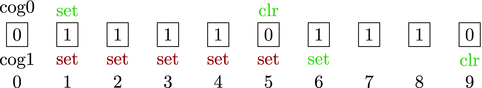
The semaphore
is created, and then a lockset/lockclr pair of instructions brackets the critical section of code. So, for example, in our code, cog 0 could acquire samples between times 1 and 5, but we must prevent cog 1 from attempting to compress them during that time. Between times 6 and 9 the compression can safely proceed.
The way we have written the code, there is in fact no chance of a collision between sample acquisition and compression. The main cog blocks while the compression cog is working, so it is impossible for it to modify sampsBuf. However, that isn’t very good design. It is wasteful for main to sit there twiddling her thumbs while steim is off doing his job. She could be (and usually is) performing other tasks. It is under that type of system design that the semaphore is most useful. After all, if one has a multicore parallel machine, we might as well use it as a…multicore…parallel…machine!
7.7.2 Using Locks for Logging
We could, for example, use a semaphore
to signal between cogs. If you don’t want to waste an I/O line for the REQ signal between cogs for logging, you could use a semaphore instead, as shown here in Listing 7-10:
1 PUB MAIN
2
3 ...
4 logSem := locknew
5 repeat until not lockset(logSem) 'acquire semaphore
6 COMPR.START ' start the pasm cog
7 ...
8
9 lockclr(logSem) ' release the semaphore, allowing PASM access
10 repeat
11 waitpne(CSMASK, CSMASK, 0)
12 logVal := READ_SPILOG
13 waitpeq(CSMASK, CSMASK, 0)
14 repeat until not lockset(logSem) ' re - acquire semaphore
15 UARTS.STR(DEBUG, string(" Log value : "))
16 UARTS.HEX(DEBUG, logVal, 8)
17 UARTS.PUTC(DEBUG, CR) ' release semaphore
18 lockclr(logSem)
Listing 7-10
Demonstration of using locks for SPI signalling
- Lines 4–9: Create a new semaphore, acquire it, and start the PASM cog. When ready to start logging, release it.
- Lines 11–13: Read a log value on the SPI lines.
- Line 14: lockset will return TRUE if somebody else has the token. In that case, repeat until won’t exit. Eventually, the other person will release the semaphore, lockset will return FALSE, repeat until will terminate, and control will continue.
- Lines 15–18: We now have the token and can slowly print out the log value, confident that the PASM cog won’t try to send another value.
- Line 18: Release the semaphore so that the PASM cog can acquire it when it is ready to send another log value.
This is the code in the Spin section that interfaces with the locks (Listing 7-11).
1 ' in the pasm cog, we must somehow pass the semaphore number (logSem)
2 ' to the cog: _clogSem
3 ...
4
5 WRITE_SPI
6 :semLoop ' acquire semaphore
7 lockset _clogSem wc
8 if_c jmp #:semLoop
9
10 ' <<WRITE LOG VALUE TO SPI >>
11 lockclr _clogSem ' release semaphore
Listing 7-11
Spin code that uses locks to signal SPI communications
- Lines 6–8: In the PASM cog, the WRITE_SPI function will check whether the semaphore is free. If so, it will acquire it, confident that the Spin cog is ready.
This loop will repeat as long as somebody else has the token. When nobody else has the token, C=0, and we continue to transmit the log value on the SPI lines.
- Line 8: Once we are done, release the semaphore.
7.8 Some Common Tasks
Here are some examples of common operations, with both Spin and PASM equivalents shown. As can be seen, some things are much simpler in Spin. This must be weighed against the speedup that can be achieved with PASM.
7.8.1 Assignment
Spin | PASM |
|---|---|
x := 42
y := 31415926
|
mov _cX, #42
mov _cY, _cbigNum
_cbigNum long 31415926
|
7.8.2 Multiplication
Spin | PASM |
|---|---|
z := x * y
|
1 shl _cX, #16
2 mov r0, #16
3 shr _cY, #1 wc
4 :loop
5 if_c add _cY, _cX wc
6 rcr _cY, #1 wc
7 djnz r0, #:loop
|
The multiply code is from Appendix B of the Propeller manual. Two 16-bit numbers, _cX[0..15] and _cY[0..15] are multiplied, and the result is saved to _cY.
Let x = 42 and y = 2. Here are their binary representations: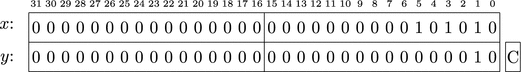
After shl _cX, #16, here is what they look like: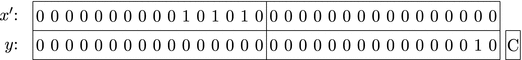
After shr _cY, #1 wc, here they are again:
Loop 1 of 16
Because C=0, the add is not performed
.
After rcr _cY, #1 wc, here is what they look like: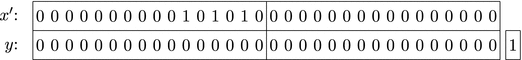
Loop 2 of 16
Because C=1, the add is performed
. The add has a wc effect, which will set C if the add overflows. In this case, C=0.
Here they are after the add: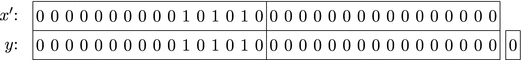
Here is the y register after rcr (the x’ register is unchanged):
From here on, y is shifted right once each iteration of the loop. No more adds are performed as all the remaining bits of y (bits 0–13) are 0.
Loop 16 of 16
The final result is y = 42 × 2 = 84.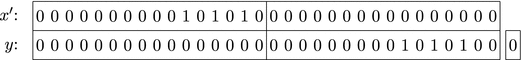
7.8.3 Division
Spin | PASM |
|---|---|
q := x / y 'quotient (32 bit)
r := x // y 'remainder (32 bit)
|
1 ' Divide x [31..0] by y [15..0]
2 ' (y [16] must be 0)
3 ' on exit, quotient is in x [15..0]
4 ' and remainder is in x [31..16]
5 ' get divisor into y [30..15]
6 shl _cY, #15
7 ' ready for 16 quotient bits
8 mov r0, #16
9 :loop
10 ' y =< x? Subtract it,
11 ' quotient bit in c
12 cmpsub _cX, _cY wc
13 ' rotate c into quotient,
14 ' shift dividend
15 rcl _cX, #1
16 ' loop until done
17 djnz r0, #:loop
18 ' quotient in x [15..0],
19 ' remainder in x [31..16]
|
This is also from the appendix. Get a pad of graph paper and confirm for yourself how it works.
7.8.4 Loops
Spin | PASM |
|---|---|
1 x0 := 0
2 x := 1
3 repeat 8
4 f := x + x0
5 x0 := x
6 x := f
|
1 mov _cx0, #0
2 mov _cx1, #1
3 mov _cf, _cx1
4
5 mov r0, #8
6 :loop
7 add _cf, _cx0
8 mov _cx0, _cx1
9 mov _cx1, _cf
10
11 mov _clogVal, _cf
12 call # WRITE_SPI
13 djnz r0, #:loop
|
The critical parts are mov r0, #8, which sets the loop counter and djnz r0, and #:loop, which decrements r0 and jumps to :loop if the result is nonzero. When r0=0, continue past the loop.
7.8.5 Conditionals
Spin | PASM |
|---|---|
if x => 10
x := 0
' else
|
1 cmp _cX, #10 wz, wc
2 if_nz_and_nc jmp #:cont
3 mov _cX, #0
4
5 :cont
6 'else
|
The compare sets the Z flag if X ≡ 10 and the C flag if X < 10. So, if neither is set, then X must be greater than 10. The if_nz_and_nc jmp #:cont instruction will jump to :cont in that case.
7.9 Summary
Setting and reading pins are central tasks to the function of the Propeller. In PASM code you set and read pins by writing to the outa register and reading from the ina register, respectively. In general, you define a mask that is specific to a pin and then operate on that mask and the ina/outa registers.
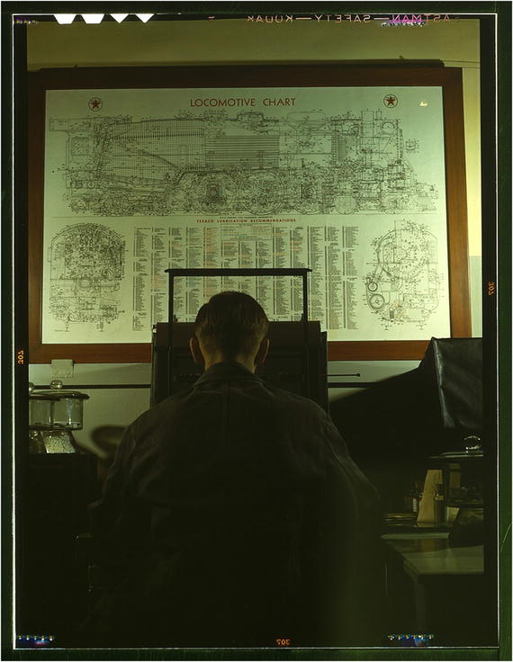
In this book I try and document my code with comments and descriptive variable and method names. In addition I use TDD when possible. In Figure 7-7, is a picture of all the lubrication points on a locomotive: documentation and maintenance!
1 mov dira, #0 wz ' set all pins to input, and set z=1
2 ' mux <flag > <dest >, <source >
3 ' the mux__ instructions set the bits of
4 ' the <destination register > that are called out in the
5 ' <source register > baseed on the value of <flag >
6 '
7 ' for example, here we set outa based _coutMask
8 ' and NOT Z (!Z)
9 muxnz outa, _coutMask
10 ' here we set dira based on _coutMask and Z
11 muxz dira, _coutMask
12
13 ...
14 ' here we toggle the bit in outa based on _coutMask
15 xor outa, _coutMask
16
17 ...
18 ' here we set C from ina, based on the value of _cinMask
19 test _cinMask, ina, wc
Figure 7-7
Locomotive lubrication chart, Chicago and NW Railroad Laboratory, Chicago, IL. Photo by Jack Delano, 1942. From the Library of Congress Farm Security Administration archives.
www.loc.gov/pictures/item/fsa1992000662/PP/
.
Footnotes
3
I lie. In reality, cog 0 would have released the cog at time 5, and during the next clock cycle, cog 1 would have requested and received the lock, but for illustration purposes, I fibbed.