
This chapter examines input devices with mechanical contacts. Switches, buttons, relays, and rotary controls all have contacts that cause trouble for electronic circuits; electronic circuits are so fast that they see contacts make and break thousands of times per second. If you ignore this aspect of input controls in your design, you could wind up with dysfunctional custom controls for your Pi.
This chapter looks at two major approaches to this problem. The first approach applies hardware, while the second is related to software. Figure 5-1 illustrates the hardware solution. Either of these methods can be successfully applied to your own Raspberry Pi custom controls.
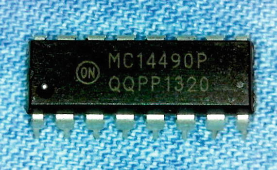
Figure 5-1. The MC14490 dual inline package (DIP) chip
Hardware: MC14490
Several potential hardware solutions are possible, but one of the best approaches uses a low-cost IC designed for the purpose. While the part is now considered obsolete, it is still available from various suppliers including eBay ($1.12 with free shipping). Keep in mind that this 16-pin DIP provides debouncing for six inputs. At 17 cents per input, the price is right!
The MC14490 is a CMOS device and can operate from 3 volts up to 18 volts. This makes it an easy sell for Pi projects using the +3.3V power supply. Finally, only one external component is required, making this an easy chip to wire up or breadboard. Be sure to take this chip for a test run.
Figure 5-2 shows the basic circuit with the debounced outputs AOUT through FOUT available for reading directly into Pi GPIO input ports. Also shown in the diagram is the +3.3V regulated Pi power to pin 16 (V DD ) and the power grounded at pin 8 (V SS ). In normal operation, the chip requires much less than 1mA and will not stress your Pi’s supply in the least.
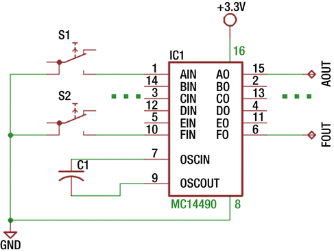
Figure 5-2. MC14490 circuit with up to six inputs and debounced outputs
Two switches (or buttons) are shown in the figure, with S1 connected to signal AIN and S2 connected to FIN. These are the inputs to AOUT and FOUT, respectively. An additional four inputs could be added to the unused pins. Normally CMOS requires that every input be connected so that it is not left floating in voltage. The MC14490 chip is designed, however, with a built-in pull-up resistor for every input. This makes the addition of resistors to the circuit unnecessary. This also allows the unused inputs to be left unconnected. Input pin 7 will have a capacitor attached to it.
Chip Operation
The MC14490 chip is marvelously simple in operation yet very effective. The datasheet for the device illustrates a block diagram consisting mainly of a 4-bit shift register, a  -bit delay, and a clock circuit. Each of the six input lanes consists of the same logic.
The operation of the device can be understood more easily in simpler human terms. At each device clock pulse, the current input is compared against the last shifted in input value. If the values differ, the shift register is cleared, and the process starts over. In this way, any bouncing of the contacts will keep clearing the shift register, and no change at the output will occur.
However, if after multiple clock pulses there is no change seen in the input value, the input level bits eventually make it out of the  -bit shift register. Once this happens, the debounced output appears on the output pin. That is the procedure in a nutshell.
In reality, the operation is a little more complicated because the shift register clear is actually implemented as a “load” operation. It must set bits all to 0s or all to 1s, depending upon the current state of the output. By doing this, the debounce process works for a signal going high and for one going low.
Capacitor C1
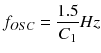
The frequency of the clock is determined by the value chosen for C
1. The ON Semiconductor datasheet lists formulas to use for various voltages. The lowest voltage formula given is for 5V operation, as shown here, where the value of C
1 is given in microfarads (μF):
I tried to estimate it for 3.3 volts, but the relationship is not linear across voltages. So, I tried some sample capacitors and hooked up the chip’s pin 9 (OSC out ) to a frequency counter (Figure 5-3). Using the results in Table 5-1, you won’t need to do the same.
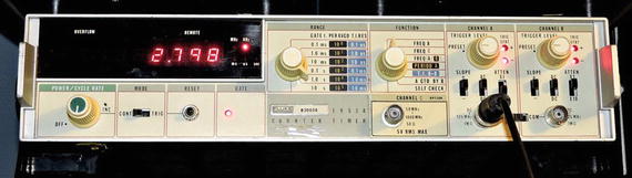
Figure 5-3. An old Fluke 1953A frequency counter used to determine the 3.3V formula for C1, by measuring frequency
Table 5-1. Experimental Frequency Readings for C1 at 3.3 Volts
C1 | Frequency | Computed K | Debounce Period |
|---|---|---|---|
0.02μF | 20Hz | 0.40 | 225ms |
0.01μF | 44Hz | 0.44 | 102ms |
0.00056μF | 797Hz | 0.44 | 5.65ms |
0.00022μF | 1916Hz | 0.42 | 2.35ms |
0.00015μF | 2798Hz | 0.42 | 1.61ms |
The factor is computed by rearranging the equation given by the datasheet, as shown here:
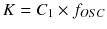
So, the factor is determined by simple multiplication. When the factor K is computed for each Table 5-1 row, it seems a value between 0.42 and 0.44 works. The fact that they tend to be all about the same value suggests that there is a solution. Now you can compute the approximate frequency for a 3.3V operation with K=0.42, as shown here:

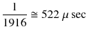
The datasheet tells you that a stable debounced output occurs in  -bit shifts. If you used a C
1 value of 0.00022μF, then your clock frequency is rather high at about 1916Hz. For a frequency of 1916Hz, each cycle takes the following:
-bit shifts. If you used a C
1 value of 0.00022μF, then your clock frequency is rather high at about 1916Hz. For a frequency of 1916Hz, each cycle takes the following:
Multiplying that figure by 4.5 times gives you about 2.35ms. That is a rather short debouncing period. Scratchy contacts can require up to 50ms of settling time. Using a value of 0.01μF reduces the clock frequency to 44Hz, which provides a debounce period of 102ms. That should more than suffice for the scratchiest of metal contacts.
Experiment
Wire up your Raspberry Pi using a breadboard and the MC14490 chip according to Figure 5-4, except leave the connection between AO on the chip disconnected from the Pi GPIO#16. Attach a Dupont wire to the Pi’s GPIO#16, while leaving the other end unconnected. You’re going to play with that wire.
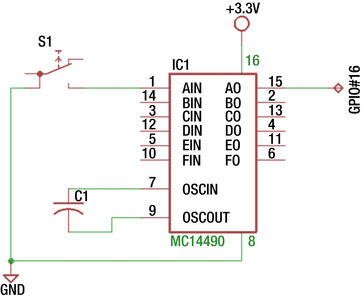
Figure 5-4. One debounced input hooked up to the Raspberry Pi on GPIO#16
Choose a suitable capacitor C 1. I recommend you use 0.01μF or slightly less. This value should be fairly responsive and yet immune to bouncing contacts.
Using the gp command, which was installed as part of the software in Chapter 1, monitor the GPIO input pin 16. Select GPIO#16 (-g16), configure it for input (-i), enable the pull-up resistor (-pu), and monitor that pin forever (-m0), until you hit Control-C.
gp -g16 -i -pu -m0Monitoring..000000 GPIO 16 = 1000001 GPIO 16 = 0000002 GPIO 16 = 1000003 GPIO 16 = 0000004 GPIO 16 = 1
Once the gp command is monitoring, the session output shows the result of scratching your GPIO#16 wire to ground. You might see several hundred changes in the output. This is what your software would see if you placed a scratchy metal contact button on that input. Now let’s let the MC14490 work its magic.
Note
While it is safest to make circuit changes when your Raspberry Pi is shut down and off, this is time-consuming and inconvenient. With care, some circuit changes can be performed while the power is applied and the Pi is running. However, applying or removing power to breadboarded chips is asking for trouble. It is recommended therefore to wire power connections when the Pi is shut down and off.
Connect the GPIO#16 to the AO output of the MC14490 (pin 15). Next attach another Dupont wire to the MC14490 AIN input. Now try scratching that wire to ground, off and on. Do you get nice clean 1 and 0 outputs?
If you don’t see it working, then check that the capacitor is properly wired in. Don’t use extremely high-valued capacitors like 1 or more μF (in fact, high-valued capacitors may ruin the chip at power off/on). If your oscillator is operating at a very low frequency, you may have to hold the change for a long time to see the output change. On the other hand, if your changes are occurring immediately, then perhaps the oscillating frequency is too high, providing very short debouncing periods. If still no joy and you lack an oscilloscope or logic analyzer, try the PiSpy program from the book Exploring the Raspberry Pi 2 with C++ (Apress, 2016).
With the circuit performing correctly, you can hook up a push button like the one illustrated in Figure 5-5. This is a simple button that I found to be bad for bouncing contacts. Attached directly to the GPIO input without debouncing, this button is simply unusable.
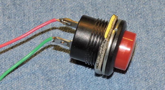
Figure 5-5. A cheap scratchy push button, with two wires soldered to it
Attach one wire of the push button to ground and the remaining one to the debouncing input AIN (pin 1). Keep the gp command monitoring (or restart it), and now when you press and release the button, you should get clean, distinct 1 and 0 events. Make sure you push the button with enough force if you don’t see any events. Sometimes these cheaply made buttons don’t function well.
More Inputs
You can’t have too many inputs, and clearly six are not always enough. For the price of another MC14490 chip, you can easily add six more debounced inputs. You don’t even need the extra capacitor.
The schematic in Figure 5-6 illustrates how IC1’s oscillator output can be shared with IC2. Both debouncing chips will run at the same frequency and reduce the number of capacitors needed.
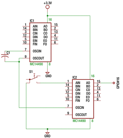
Figure 5-6. Two MC14490 chips sharing one oscillator
The schematic can be wired up on your breadboard and tested. Here you move the push button to IC2’s AIN and connect the Pi’s GPIO#16 to IC2’s debounced output on pin 15. Wire it up and test it as before to satisfy yourself that this works.
Figure 5-7 shows the two ICs connected to share one oscillator. The scratchy push button was moved to IC2 to prove that it too operates correctly.
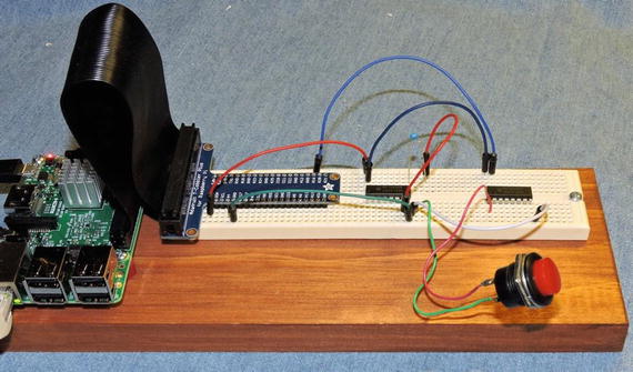
Figure 5-7. Two MC14490 chips sharing one oscillator, interfacing with GPIO#16
If you download and read the ON Semiconductor datasheet, you’ll find that it is possible to do some other tricks with the MC14490. For example, if you use two debouncers and a NOR gate, you can have one input produce a pulse when the button is pressed. This is useful when you need a pulse, even when the end user holds the button down without releasing it.
Software Debouncing
I’ve discussed one hardware solution in this chapter, but if you don’t mind expending some CPU cycles, you can do the same work in software. Here is one fairly simple approach for software:
Clear your program state by reading the GPIO input (as v) and then doing one of the following:
Set shiftr to 0 if the input v is a 0 bit.
Set shiftr to all 1 bits when the input v is a 1 bit.
At the top of the loop, read the GPIO pin (again) into variable b.
Shift shiftr left one bit, and set shiftr.bit_0=b.
Examine the lower four bits of shiftr.
Are they all 0 bits? Set s=0.
Are they all 1 bits? Set s=1.
If they’re neither all 0 bits or all 1 bits, repeat the exercise starting with step 2.
If s = v, then there is no change. Repeat the exercise starting with step 2.
If s ≠ v, then you have a debounced change in signal. Continue with step 7.
Now set the debounced signal as v = s.
Repeat the loop with step 2.
The idea is that you keep shifting bits into a shift register (shiftr) at regular intervals. When the input stays high or stays low, the bits shifted into the register will all be the same.
Let’s use a concrete example, using eight bits to hold shiftr to illustrate the procedure.
00000000: This is the initial value of shiftr. You also assume that the debounced state is 0.
00000001: The bit shifted in from the right indicates that the input line went high.
00000010: Because of bouncing contacts, you shifted in the next read value, which is low.
00000101: Because of bouncing, the next read value was a high value.
00001011: Read another high value.
Steps 2 through 4 have sampled the input line four times now. But the low-order bit pattern is currently 1011, which is neither all 1 bits nor all 0s. So, you don’t register any debounced change in value.
00010111: Read another 1 bit (line still high). The low-order bits are 0111, which still does not represent a debounced change.
00101111: Read another 1 bit (line still high). Now when you look at the low-order bits, you see 1111. Because the saved state is 0, this represents a change to the 1 state. You now can set the debounced state to 1.
From the concrete example, you see that nothing changes until the requisite four lower bits are all 1s. Now as long as you keep reading 1 bits on the line or even mostly 1 bits, the state will never leave the debounced state of 1.
After a while, the user is going to flip the switch to the opposite state (in this case, grounding the input).
01011110: Read a 0 bit (the line has gone low).
10111101: Read a 1 bit because of bouncing contacts.
01111010: Read a 0 bit (the line has gone low again).
11110100: Read another 0 bit. The lower four bits are 0100, which is nothing special.
11101000: Read another 0 bit. There’s still nothing special about the lower four bits.
11010000 Read another 0-bit. Now the low-order four bits are 0000. This indicates a debounced zero level.
Now you have reached the debounced state for zero.
Whenever the signal waffles between 0 and 1, it pollutes the bit pattern in the shift register so that no action is taken. However, when the signal stabilizes, the bit pattern will be either 0000 or 1111. If the state differs from the pattern, you know that you have a debounced transition.
In this example, I am assuming that you needed four bits. This was arbitrary and inspired by the MC14490 design. I have used three, four, or even five bits depending upon the sampling period and the response time required for various projects.
Experiment
To perform the software signal debouncing experiment, wire up a scratchy push button to your Raspberry Pi, as shown in Figure 5-8.
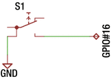
Figure 5-8. Software push button debouncing experiment
Change to the debounce subdirectory and type make if the software has not yet been compiled yet. This will create the executable program debounce. Run it as follows, once you have the push button wired up:
$ ./debounceNow debouncing gpio_pin = 16. ^C to exit.State changed: 1State changed: 0State changed: 1State changed: 0State changed: 1State changed: 0State changed: 1^C
This session shows several push button presses and releases. Did your scratching push button work like a good one?
Listing 5-1 shows the software listing for debounce.cpp. Lines 016 to 027 of the main program configures GPIO#16 as an input, with the pull-up resistor applied. The pull-up resistor is necessary so that when the push button is not pressed, the open circuit allows the resistor to pull the GPIO line high. Otherwise, the GPIO line would float and sometimes read high and sometimes low. Not a happy situation!
Line 031 initializes the state variables. The value of state just tracks whether the debounced output is high or low. Variable shiftr is the shift register, loading the most recently read bit into the variable from the right (bit 0). Value b is the most recently read bit from GPIO#16.
Line 036 shifts the most recently read bit from the GPIO into the shift register. Old bits are simply shifted out of the register. Line 037 is where the value of m is assigned the lowest four bits from the shift register.
Things get interesting in line 039 where m is tested to see whether the bit pattern is 0000 or 1111. If one of those patterns applies, line 040 tests to see whether the low-order bit matches the current state. A state change occurs only if the line value differs from what you already have established. If there is indeed a change of state, execution proceeds to line 041 where the new state is saved and a message is printed, for demonstration purposes.
Listing 5-1. The debounce.cpp Software Debouncing Program
001 // debounce.cpp002003 #include <stdio.h>004 #include <unistd.h>005 #include <stdlib.h>006 #include <string.h>007 #include <errno.h>008009 #include "gpio.hpp"010011 static int gpio_pin = 16; // Input012013 static GPIO gpio;014015 int016 main(int argc,char **argv) {017 int rc;018019 if ( (rc = gpio.get_error()) != 0 ) {020 fprintf(stderr,"%s: starting gpio (sudo?)\n",strerror(rc));021 exit(1);022 }023024 gpio.configure(gpio_pin,GPIO::Input);025 assert(!gpio.get_error());026 gpio.configure(gpio_pin,GPIO::Up);027 assert(!gpio.get_error());028029 printf("Now debouncing gpio_pin = %d. ^C to exit.\n",gpio_pin);030031 int state = 0, shiftr = 0, m, b;032033 for (;;) {034 b = gpio.read(gpio_pin); // Read bit035036 shiftr = (shiftr << 1) | (b & 1);037 m = shiftr & 0b00001111; // Mask out low order bits038039 if ( m == 0b00001111 || m == 0b00000000 ) {040 if ( (shiftr & 1) != state ) {041 state = shiftr & 1;042 printf("State changed: %d\n",state);043 }044 }045 usleep(10000);046 }047048 return 0;049 }
Before the loop repeats, you pause the program’s execution in line 045, with a delay of 10,000μsec (10ms). This step is necessary for two reasons.
Without the delay, the CPU would be consumed in a tight execution loop. This is not only wasteful but will cause your Pi to consume more power and get warmer (did you purchase a heatsink for your Pi 3?).
You look only at the four lower bits in the shift register (shiftr). If you want to debounce about 40ms of contact bounce and perform this in four samples, then you need to sample about 10ms apart.
So if you want more samples, or quicker response, play with the number of bits and the delay time.
Summary
The MC14490 is a great little chip when you need a hardware solution to debouncing input contacts. These contacts could come from switches, buttons, relays, or reed relay contacts. With the information provided, you will be able to apply this chip at 3.3 volts to the Raspberry Pi and pick the correct capacitor for the type of response you need.
If, however, you decide upon a software solution for debouncing, then the code in this chapter provides a working solution for you.