Looking through online forums, I often see posts from people struggling with how to interface between 3V and 5V logic systems. Advice varies widely, ranging from “connecting it directly seems to work for me” to other dubious methods.
The purpose of this chapter is to eliminate the guesswork. The solutions presented here are not the only solutions available, but they are practical for those seeking answers. I’ll focus specifically on 3.3V and 5V systems in this chapter because the Pi is a 3V system and a great many parts still use 5 volts.
To be clear, this chapter is about signal interfacing, not driving high-powered loads. Power introduces other factors that go beyond signal interfacing. I2C also does not apply here because of its bidirectional nature and the use of the open collectors. Signal interfacing does, however, apply to GPIO-, TTL-, and SPI-related circuits. Figure 2-1 illustrates some of the featured components used in this chapter.
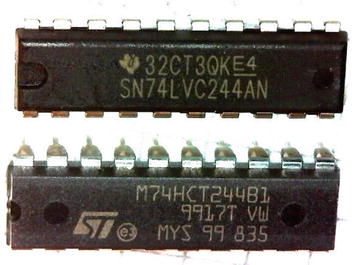
Figure 2-1. Two useful level interfacing chips
7400 Series (TTL)
The 7400 series of integrated circuit (IC) was developed in the 1960s and 1970s to be used as building blocks for digital mainframe computers (the 5400 series is the military-grade equivalent). This is known as transistor-to-transistor logic (TTL), which largely replaced the earlier diode transistor logic (DTL).
TTL circuits use a 5V power supply (usually referred to as VCC) and use defined voltage ranges for what is considered true (1) or false (0). Any signal that is between these ranges is considered undefined or ambiguous.
Since these digital signal levels are measured by voltage and because the signals of interest are input or output signals, they use the symbolic notation shown in Table 2-1.
Table 2-1. Signal Symbols
Symbol | Description |
|---|---|
VI | Voltage of an input |
VO | Voltage of an output |
Input and output ranges are further qualified using the symbols in Table 2-2.
Table 2-2. Input and Output Signal Symbols
Symbol | Description |
|---|---|
VIL | Voltage of an input, at low level |
VIH | Voltage of an input, at high level |
VOL | Voltage of an output, at low level |
VOH | Voltage of an output, at high level |
When we begin with logic levels, we must start with input logic levels. These levels decide what is considered a 0 or 1 when received from the sending circuit. Thus, the signals of primary interest are VIL and VIH . Look for these when examining a datasheet (you usually can find a datasheet for a given chip by Googling <part-number> datasheet PDF).
Table 2-3 describes the TTL (5V) levels. Notice that VIH is defined in terms of VCC for its highest voltage range. Remember also that VCC can itself vary by up to 10 percent in value because the power supply varies. When VCC varies like this, VIH can be as low as 4.5 volts or as high as 5.5 volts.
Table 2-3. TTL (5V) Input Logic Levels
Symbol | Minimum | Maximum | Description |
|---|---|---|---|
VIL | 0.0 volts | 0.8 volts | Logic value false (0) |
VIH | 2.0 volts | VCC | Logic value true (1) |
It is clear from Table 2-3 that any digital signal from 0.0 volts to 0.8 volts is to be considered a false (0) input. Signals at 2.0 volts or higher are considered true (1). Any voltage between these levels is ambiguous and must be avoided. Ambiguous levels are interpreted unpredictably as 0 or 1.
Generating an exact voltage level consistently and reliably is difficult, if not impossible. For this reason, ranges of acceptable values are used. For example, if your digital input signal is 0.125 volts, it clearly falls within the TTL logic 0 range. In another example, a voltage input of 2.8 volts is clearly interpreted as a logic 1.
When you examine output signals, the output needs to meet the requirements of the input ranges if the signal is to reliably transmit digital data. For example, if a hypothetical part generates logic 1 output voltages between 3.0 volts and VCC, then it meets the TTL interface requirements for logic high. This is because 3.0 volts meets and exceeds the 2V minimum. If the same part is guaranteed to generate logic low levels between 0.1 and 0.6 volts, then this clearly falls into the TTL low range also. With these voltage ranges, this part will successfully communicate with other TTL component inputs.
3.3V Logic
With the introduction of complementary metal-oxide semiconductor (CMOS) logic soon after TTL, a definition for CMOS logic levels had to be agreed upon. The difficulty with CMOS, however, was that it could operate over a range of different power supply voltages (note that the power supply is often referred to as VDD for CMOS). For this reason, CMOS logic levels are usually defined in terms of the operating VDD instead. Fractional values are provided in [1], while the percentage references can be found in [2].
Table 2-4 lists the CMOS logic level guidelines.
Table 2-4. CMOS Logic Levels
Symbol | Minimum | Maximum | Description |
|---|---|---|---|
VIL | 0.0 volts | 1/3 VDD | Logic value false (0) |
30% VDD | |||
VIH | 2/3 VDD | VDD | Logic value true (1) |
70% VDD |
The CMOS ranges provided in Table 2-4 are approximate. The final range is defined by the device’s datasheet.
Even though the Raspberry Pi CPU is CMOS-based, the input specifications provided by Broadcom are slightly different and documented in Table 2-5.
Table 2-5. Raspberry Pi Logic Levels
Symbol | Low | High | Description |
|---|---|---|---|
VIL | 0.0 volts | 0.8 volts | Logic value false (0) |
VIH | 1.3 volts | VDD | Logic value true (1) |
In this chapter, you will have to pay attention to all three sets of input logic levels.
I’ve introduced several symbols and voltage levels. Figure 2-2 will help you visualize what I am about to discuss. For now, ignore the fact that the 5V signal exceeds the supply voltage for the 74LVC245. This will be explained later.
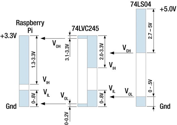
Figure 2-2. Example of logic level conversion
On the right side of Figure 2-2 is an example 5V TTL device (74LS04). In the middle is the level shifting device. Finally, on the left is the Raspberry Pi GPIO input that I want to feed a signal into.
The signal starts at the output of the 74LS04. According to its datasheet, the output is never lower than 2.7 volts when it represents logic 1 and never higher than 0.5 volts when it represents logic 0. These are the 74LS04 device’s VOH and VOL output levels, respectively. The arrows from the 74LS04 pointing left show how these voltage levels are passed into the left device’s inputs. Whether the left device sees a logic 1 or 0 depends upon its own input level definitions VIH and VIL. In the Figure 2-2 example, you can see that the 74LS04 clearly exceeds the 74LVC245 input requirements.
The middle device is illustrated with these two sets of parameters:
Input levels VIL and VIH
Output levels VOL and VOH
When examining interfaces, you must remind yourself that the input and output voltage levels differ. The output levels must exceed the input levels of the receiving device (if they only just met the requirement, there would be no “noise margin” of safety).
Examining the 74LVC245 device going left to the Pi, you must meet the Pi’s slightly different input parameters. Following the arrows going left, you can see that the 74LVC245 output levels definitely exceed the Pi’s input requirements. This is the general principle of level shifting from an output to an input.
Voltage Dividers
Converting from a higher to a lower voltage logic can sometimes be done using a pair of resistors in a voltage divider configuration (Figure 2-3). This can be attractive when there are only one or two signals involved. But this quickly becomes burdensome when the number of signals increases because of the parts count.
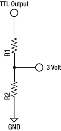
Figure 2-3. Voltage divider circuit
A pair of resistors wired in series can take a worst-case 5V signal and produce a 3V level by dividing the voltage. The values of the resistors are chosen from a ratio, as shown here:
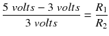
The basic idea is that you make 3 volts appear across R2 but drop the remaining 2 volts across R1.
The first problem is that you must choose a value for R1 or R2 before the resistance can be solved. But if you choose too high a value, then any current flowing into or out of the midpoint junction will cause its voltage to vary (the divider is not “stiff” enough). The rule of thumb is that the series current through R1 and R2 should be at least ten times any incoming or outgoing current from the junction. The added current flow will stiffen the divider.
The Pi’s CMOS input requires nearly zero current. The only current that does flow is when there is a change of state, requiring a small charge or discharge to occur. This charge transfers to/from the stray capacitance at the chip’s pin and the CMOS gate. Engineering students can compute this tiny charge as an exercise, but here I’ll suggest that 1mA is plenty of “stiffness.”
Resistors come in different tolerances. You can assume the following 10 percent resistor values for this example:


If you were to do all the Ohm’s law math, you’d discover that the midpoint voltage (VR2) would be 2.97 volts when the TTL input is 5 volts.
Let’s test this arrangement using a Texas Instrument 74LS04 output feeding into the voltage divider. The divider’s output will be used as an input for the Raspberry Pi. You want to test whether this will actually work under all possible conditions.
Assume a worst-case 74LS04 output low voltage of VOH=0.5 volts, and assume VOH=2-7 volts for output high. These represent the datasheet’s guaranteed worst-case figures. Table 2-6 summarizes how the voltage divider measures up. The column “Pi Margin” measures the difference between the Pi’s requirement and the value appearing at that input.
Table 2-6. Voltage Divider from 74LS04 to Pi
Symbol | TTL | Divider | Pi Margin | Description |
|---|---|---|---|---|
VOL | 0.4 volts | 0.24 volts | 0.56 volts | Logic value 0: 0.56 volts under the limit |
VOH | 2.5 volts | 1.49 volts | 0.19 volts | Logic value 1: 0.19 volts over the minimum |
From Table 2-6 you can see that VOL is below the Raspberry Pi requirement of 0.8 volts by a margin of 0.56 volts. The worst case for the 74LS04 output high (VOH) has a lower margin of 0.19 volts over the Pi’s minimum of 1.3 volts. It appears that you’ve met the requirements, even though a bigger safety margin on the high side is desirable.
Is the circuit acceptable if you consider the worst-case values for the 10 percent resistors R1 and R2? Recall that I used a parts tolerance of 10 percent. The worst case here would be R1 + 10 percent and R2 – 10 percent because this would lower the midpoint voltage further. Table 2-7 summarizes this result.
Table 2-7. Results of Worst Case 10 Percent Resistor Error
Symbol | TTL | Divider | Pi Margin | Description |
|---|---|---|---|---|
VOL | 0.4 volts | 0.22 volts | 0.58 volts | Logic value 0: 0.58 volts under the limit |
VOH | 2.5 volts | 1.36 volts | 0.06 volts | Logic value 1: 0.06 over the minimum |
It is clear from Table 2-7 that the VOH result of 1.36 volts is dangerously close to the absolute limit of the Raspberry Pi specification (1.3 volts). The margin of error is only 0.06 volts. This is looking shaky.
From this, you might conclude that the voltage divider is not as attractive as it might first appear. From a hobby perspective, you can make this work by cherry-picking your resistors carefully or by using lower-tolerance resistors. What you didn’t consider was that the power supply can vary by another 10 percent in its supply voltage. If you were to turn this into a product (or a kit), you’d want to improve that error margin to avoid shipping faulty units.
Finally, consider also that this analysis is sensitive to the TTL part that is being used. If you substituted the 74LS04 for a part with poorer worst-case conditions, you may end up generating signals that are “out of spec.”
7400 Series Derivative Families
The 74L low-power series was introduced in 1971, which was soon superseded by the faster 74LS series. Several new series derivative families began to appear including 74H (high speed), 74S (high speed Schottky), and so on. Finally, CMOS-compatible families were added including HC and HCT. Currently several derivative families are available [3].
Table 2-8 lists some of the derivative families that may be of interest. We’ll focus on the HCT series and LVC series derivative families. While other families may sometimes work, you must also consider the speed of the device, particularly when you want to do high-speed SPI, for example.
Table 2-8. Some 7400 Series Derivative Families [1]
74XX Series | Description |
|---|---|
HC | High-speed CMOS, similar performance to LS, 12ns, 2.0–6.0 volts |
HCT | High-speed, compatible logic levels to bipolar parts |
AHCT | Advanced high-speed CMOS, three times as fast as HC, tolerant of 5.5V on input |
LVC | Low voltage: 1.65–3.3V and 5V-tolerant inputs, TPD < 5.5ns at 3.3 volts, TPD < 9ns at 2.5 volts |
LVT | Low-voltage: 3.3V supply, 5V-tolerant inputs, high output current < 64mA, TPD < 3.5ns at 3.3 volts, IOFF, low noise |
Unused CMOS Inputs
Before I present breadboard experiments using CMOS devices, you should be aware of the unused input quirk of CMOS devices. TTL devices can have unconnected inputs, even though it is usually best to ground them to avoid noise. CMOS inputs, however, must be connected.
CMOS inputs can be tied to ground or VDD. They simply must not be left “floating.” Failure to observe this practice can result in unusual behavior or potential device failure.
Converting 5V to 3V Input: 74LVC245
The LVC series derivative family can help when you want to convert a 5V signal to 3.3 volts. The first of this family that you’ll examine is the 74LVC245.
The 74LVC245 chip provides eight bidirectional buffers, with tristate capability. For a level translator, you’re not interested in the tristate or bidirectional capabilities. These can be hardwired to function in one direction only, and tristate can be disabled (some users might find the tristate useful, but the direction should be hardwired). What is of critical importance is how the configured input is transformed from the TTL level to the Pi level.
Figure 2-4 provides an abbreviated logic diagram for the buffers A1 and B1. The remaining seven buffers are controlled by the same DIR and OE gate inputs and are available on the remaining device pins.
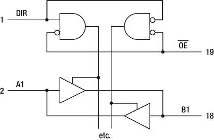
Figure 2-4. 74LVC245 octal bus transceiver
Wiring the DIR and OE gate inputs to ground causes the data to flow from input B1 to output A1. This configuration enables the buffer going from right to left, while disabling the buffer going left to right.
The 74LVC245 was chosen here because it can be supplied with +3.3 volts but can accept input voltages (at B1) at voltages as high as +5 volts. This feature is critical, since most ICs will accept only a maximum of their supply voltage (+3.3 volts) plus one diode drop (about 0.6 volts). This is because of the way electrostatic discharge (ESD) protection works in the device.
The 74LVC245 must operate at +3.3 V so that its output (A1) will provide a maximum of +3.3 volts to the Raspberry Pi. It also happens to be the recommended operating voltage for this device.
Figure 2-5 illustrates the circuit for interfacing 5V inputs (B ports) to the Raspberry Pi (A ports). The single 7404N chip (IC2A) is shown to represent some arbitrary TTL level signal wired to B1. Additional TTL signals can be wired to B2 through B8 in the same way.
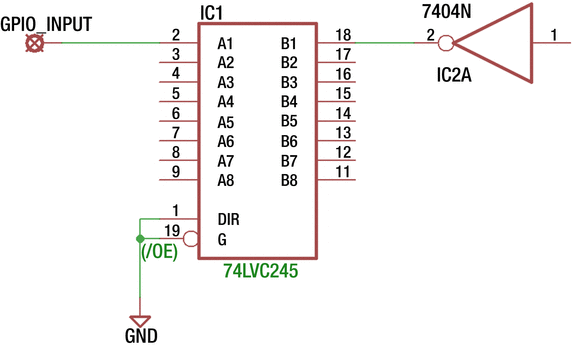
Figure 2-5. 74LVC245 as a TTL to 3V level converter
The figure doesn’t show this, but the 74LVC245 (IC1) chip must be powered from a +3.3V supply (Raspberry Pi supply). The TTL chip (IC2A), on the other hand, will be powered by the 5V supply.
Substituting a 7400 chip quad NAND gate for IC2A in Figure 2-5, its output was fed into the 74LVC245 (IC1) input B1 for an experiment. Table 2-9 summarizes the measured DC voltages.
Table 2-9. Measured 74LVC245 DC Voltages
7400 VCC | 7400 Inputs | 7400 Output | '245 VDD | '245 B1 | '245 A1 |
|---|---|---|---|---|---|
+4.99 volts | Gnd | +4.45 volts | +3.29 volts | +4.45 V | +3.29 V |
+4.99 volts | +0.038 volts | +0.38 V | +0.009 V |
Figure 2-6 shows my breadboard setup used for the measurements in Table 2-9. The lab unit shown on the left was a hamfest (ham radio flea market) deal that I scored one summer day. Hamfests are great for acquiring parts and used equipment (like the used Fluke bench DMM under the scope).
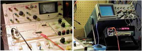
Figure 2-6. Breadboard test setup
From this test, it was observed that the 74LVC245 tolerated the +4.45V input and produced a nice +3.29V output on A1. The 3V supply was not raised, which can happen if an incorrect part is used for IC1 (because of internal protection diodes). When the TTL input of +0.38V was provided to B1, the 74LVC245 improved the VIL signal as A1=+0.009V. The 74LVC245 performed marvelously as a 5V to 3V conversion device.
Converting 5V to 3V Input: 74LVC244
The 74LVC244 device is another member of the LVC derivative family (Figure 2-7). This device has the advantage that it is unidirectional, making it simpler and potentially cheaper than the 74LVC245 device. To use this device, the two OE inputs are wired to ground to permanently enable the 3V outputs (unless, of course, you need tristate). The inputs are 5V tolerant, making this another terrific logic level converter.
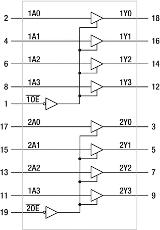
Figure 2-7. 74LVC244 pinout
Table 2-10 summarizes the measurements taken when the 74LVC244 was used.
Table 2-10. Measured 74LVC244 DC Voltages
7400 VCC | 7400 Inputs | 7400 Output | '244 VDD | '244 B1 | '244 A1 |
|---|---|---|---|---|---|
+5.02 volts | Gnd | +4.69 volts | +3.31 volts | +4.69 V | +3.31V |
+5.00 volts | +0.035 volts | +0.35 V | +0.012 V |
The experiment once again confirms that the input of the 74LVC244 was permitted to be higher than the VDD supply of +3.3 volts. Had this device not possessed this special feature, the '244 input reading might be +0.6 volts or higher. This will be clarified when I discuss protection diodes.
CD4049/CD4050
You might use the CD4049 or CD4050 CMOS devices if you don’t need high switching speed (these have a worst-case rise/fall time as high as 120ns). The CD4049 is a hex inverter, while the CD4050 has six noninverting buffers. These CMOS devices can be supplied with VDD=+3.3V to match the Raspberry Pi yet accept an input signal as high as +18 volts. When operating at +3.3 V, the VIL maximum is approximately 1.0 volts (30 percent VDD), and the VIH minimum is +2.3 volts (70 percent VDD). Given that the 7400 datasheet lists a VOH minimum of +2.7 volts, this meets the CMOS input requirements (the VOL/VIL parameters are also met).
Repeating the experiment using the 7400 quad NAND gate to drive a CD4050, you get the DC readings shown in Table 2-11. The schematic is the same as Figure 2-5, except that IC1 is the CD4050 and IC2A is one of the 7400 NAND gate outputs (with inputs wired together, to behave as an inverter).
Table 2-11. Measured CD4050 DC Voltages
7400 VCC | 7400 Inputs | 7400 Output | CD4050 VDD | CD4050 In | CD4050 Out |
|---|---|---|---|---|---|
+5.01 volts | Gnd | +4.65 volts | +3.30 volts | +4.65 volts | +3.30 volts |
+5.00 volts | +0.036 volts | +0.036 volts | +0.012 volts |
Once again, you can see that the CD4050 happily accepts a high input voltage of +4.65 volts. Had a protection (clamping) diode been involved, this voltage would be lowered to about +3.9 volts or a little more. Because the CD4050, however, does not do this kind of limiting, it works well as a level converter. Its main disadvantages are lower speed and the fact that you get only six buffers instead of eight.
Input Protection Diodes
The 74LVC245 and 74LVC244 devices were special devices because they allowed a 5V signal into an input, even when that device was operating at VDD=+3.3 volts. Let’s take a moment to understand why this is special.
The CMOS gate is a metal oxide that is deposited on a thin layer above the silicon channel where current flows. Any small voltage change exerted on that insulated gate causes a larger change in electron flow in the channel beneath. But if the electric charge is high enough, the metal oxide can be punctured and shorted out. This damage is permanent and destroys Field Effect Transistor (FET) operation.
To protect the gate from static electricity, protective diodes are built into the device. There are different ways this is accomplished, but it is frequently done as shown in Figure 2-8. Diodes D1 and D2 are reversed biased in a way that causes them not to interfere with normal input signals.
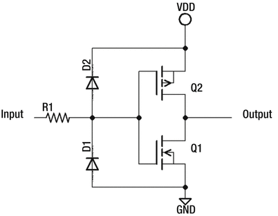
Figure 2-8. Inverter equivalent circuit
The inverter circuit shown has the FET transistors Q1 and Q2 arranged in the typical CMOS configuration. When one transistor is on, the complementary transistor is off. The input is usually guarded by a low-valued resistance R1 to limit the current flow when a static discharge occurs. Since the metal-oxide gates do not conduct electricity, the diodes D1 or D2 are designed to bleed the static charge away. By bleeding the charge away, the voltage levels are kept low enough to prevent gate puncture damage.
For the student, schematic diagrams are drawn so that diodes form an arrow of conventional current flow. That is, the current is shown flowing from plus to minus even though physicists have long ago proven that electrons flow from minus to plus. If you pretend conventional flow is correct while we look at the diagram, you can visualize the fact that no current flows from plus to minus through the diodes because they are reversed in polarity.
If you pet a cat and then come in contact with (or close to) this gate’s input, static electric current will flow from the input through D2 or D1, depending upon whether the electric charge is positive or negative. I have not been able to determine which charge it is though I have regularly snapped sparks to our cat’s ears. If you shuffle your feet on a carpet, the generated charge may be positive or negative depending upon the materials involved.
The protection diodes work rather well for static charges under normal handling conditions. The problem occurs when you want to do something like feed a 5V signal into a CMOS input when the device is operating at a supply voltage of +3.3 volts. Examine Figure 2-9, which is rearranged slightly to illustrate the high voltage flowing into a lower-voltage device’s input.
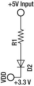
Figure 2-9. Current through protection diode D2
If the input pin of the inverter is raised to +5 volts, then the input voltage is above the chip’s own supply VDD=+3.3 volts. This difference is as follows:
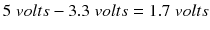
The voltage that develops across a silicon diode is usually about 0.6 volts, so you need to subtract that to arrive at the voltage across R1.
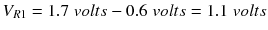
The resistance value isn’t normally provided in the datasheets but may be near 200 ohms [4]. This means that when the input signal is provided at +5 volts, the current flow through R1 is as follows:
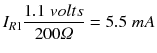
The difficulty is that you have no guarantee that the protection diode can sustain 5.5mA of current. The protection diodes are designed to discharge weak currents for brief periods of time. For this reason, you shouldn’t design a circuit to rely on its use. A similar problem exists when the input is made less than -0.6 volts (negative), causing current to conduct through D1 instead.
The special feature that permits you to provide a higher-than VDD input voltage is a protection circuit that depends upon a Zener diode for D1, as shown in Figure 2-10.
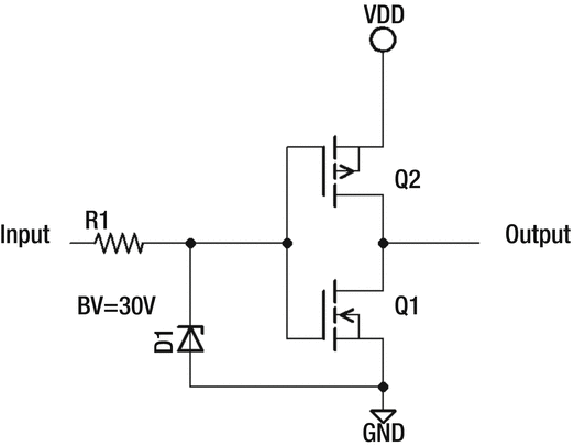
Figure 2-10. Inverter with Zener input protection
Diode D2 is no longer required because D1 is a Zener diode, which has a designed breakdown voltage in the reverse direction. The exact voltage where the Zener action occurs is not usually specified but guaranteed to occur above some absolute high value. The Fairchild Semiconductor datasheet for the CD4049UBC or CD4050BC lists the absolute maximum voltage for the inputs at +18 volts [5]. So, the Zener action must occur somewhere above that.
D1 is a Zener diode when reversed biased. It otherwise conducts current like a normal diode when forward biased. This means that if the input signal goes negative, the Zener diode starts conducting at about -0.6 volts like the normal protection diode. Thus, the single Zener diode protects against both positive and negative static charges.
From this, I hope that you can see that there is a need for this special feature. Without this adaptation to allow an input signal to exceed the +3.3V VDD level, you risk burning out a protection diode in the chip. In the datasheet, look for special mention of the ability to operate input signals above their supply voltage. The CMOS chips CD4049UBC (inverter) and CD4050BC (buffer) both possess this talent, along with the previously discussed 74LVC244 and 74LVC245 devices.
Converting 3 Volts to 5 Volts with the HCT Family
Now you can turn your attention to converting a 3V signal into the higher-level 5V signal. Here you turn to a different series family member. Previously the LVC family was used, but here you must use an HCT family.
The main reason for this is that you must power the device from 5 volts in order for it to have an output swing from 0 to 5 volts. Its outputs must match the receiving TTL input levels (VIL of 0.8 volts maximum and VIH of 2.0 volts minimum). Let’s first review the 74HCT245 device.
74HCT245
The main trick, however, is that the 74HCT245 device itself must accommodate a low enough input VIH for the driving Raspberry Pi. Normally the CMOS high level (70 percent of 5 volts) would mean a VIH of 3.5 volts. This is higher than the Pi can produce! But because the HCT family is designed to accept TTL input levels, you can count on its VIH to be 2.0 volts instead. This is the special talent of the HCT family.
To make this easier to visualize, examine Figure 2-11. Notice that the 74HCT245 is being supplied by 5 volts this time, allowing its output to range from 0 to 5 volts. Even though the input to the 74HCT245 can go as high as 5 volts, the Pi will never deliver more than +3.3 volts. This is why it is important that the VIH of the 74HCT245 is as low as 2 volts. Notice from the CMOS device on the left, sending to the '245 in the center and driving the TTL device at the right, the signal parameters are exceeded at every turn. By having this “noise margin,” a small noise blip on the signal won’t push it out of spec and cause erroneous readings.
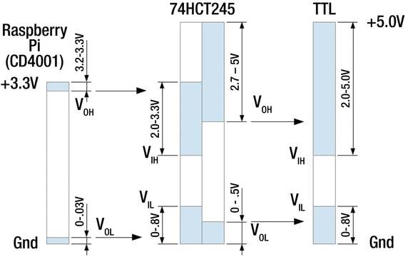
Figure 2-11. 3V CMOS to 5V TTL conversion
A couple of notes about Figure 2-11 are in order.
The VOL and VIL were estimated values for the CD4001 operating at +3.3 volts (Fairchild lists only the values for 5V operation).
The Raspberry Pi’s output parameters are expected to be similar to the CD4001, though they are not actually provided by Broadcom.
To test this in a simple manner, the circuit in Figure 2-12 was breadboarded to illustrate the signal conversion from the Pi GPIO to the TTL signal. The output of the two-input NOR gate (IC2A) is used to simulate the output of the Raspberry Pi in this experiment. IC2A is supplied by a +3.3V power supply like the Pi would supply.
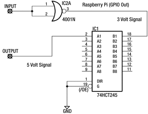
Figure 2-12. 3V to 5V conversion circuit
IC1 is the 74HCT245 device, which is powered from +5.0 volts in this circuit. This allows the output of the device to swing between 0 volts and 5 volts to drive the TTL device. The TTL input would be connected to the terminal “OUTPUT” in Figure 2-12.
Table 2-12 summarizes the experimental measurements. When the CD4001 supplied a 3V system high (+3.30 volts), the output of the 74HCT245 was +5.03 volts. When the CD4001 supplied a logic 0, the 74HCT245 supplied a low of +0.004 volts. These represent excellent results.
Table 2-12. Measured 74HCT245 Voltages
CD4001 VDD | CD4001 Inputs | CD4001 Output | 74HCT245 VDD | 74HCT245 In | 74HCT245 Out |
|---|---|---|---|---|---|
+3.30 volts | Gnd | +3.30 volts | +5.03 volts | +3.30 volts | +5.03 volts |
+5.03 volts | +0.0010 volts | +0.0010 volts | +0.004 volts |
74HCT244
The 74HCT244 is a simpler part because it is unidirectional and may be lower in cost. Again, this part must operate from +5 volts like the 74HCT245 discussed earlier. If you’re squeezing the last few microamps out in power savings, the '244 device is feeding fewer transistors internally.
The pinout is the same as the LVC part shown earlier in Figure 2-7. Simply supply your Pi inputs to the 75HCT244 inputs, and the 5V logic outputs will appear at the device outputs. Make sure that the OE pin is grounded to enable the outputs.
Switching Speed
One parameter that I have avoided discussing is the switching speed of various devices. For driving LEDs and motors, speed may not be critical. You might desire higher data rates for SPI interfaces, on the other hand. The question naturally arises, how fast can my device go?
The datasheets won’t answer this directly. They do, however, provide the following parameters:
tPHL: Propagation delay time, high to low
tPLH: Propagation delay time, low to high
The Fairchild CD4001 datasheet lists these values, as shown in Table 2-13.
Table 2-13. Fairchild CD4001 Datasheet
Parameter | Description | Value |
|---|---|---|
tPHL | Propagation delay time, high to low | 250ns |
tPLH | Propagation delay time, low to high | 250ns |
For this device, both parameters have the same times, but they need not be identical (these are the values listed for 5V operation). So, the absolute maximum speed these devices can signal from low to high and low again can be calculated as follows:
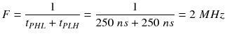
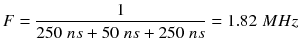
But this is not all there is to it because the signal must usually hold for a time in one state or the other. The actual rate could easily be half or less. If, for example, the high state hold time is 50ns, the rate reduces to the following:
The NXP 74LVC244 datasheet specifies in a small print note that “tpd is the same as tPHL and tPLH.” They list tpd with a maximum of 7.5ns for this device at 3.3 volts. So, what is the absolute maximum frequency for this device?
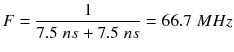
Notice the difference in signal rate. Again, this does not take hold times into account, but knowing the absolute limit is helpful in planning. As Clint Eastwood said (as Harry Callahan), “A man’s got to know his limitations.”
Summary
This chapter has been a little intense about signals, levels, voltages, and parameters. This was designed to help you understand the critical issues involved. If you don’t yet have a mastery of digital electronics, then you’d still be well served with the following simple advice:
When converting from 5 volts down to 3 volts, use the 74LVC244 device (or 74LVC245), powered by +3.3 volts.
When converting from a 3V signal up to 5 volts, use the 74HCT244 device (or 74HCT245), powered by the 5V supply.
When considering alternative devices, don’t forget to evaluate their switching speeds. Many older devices are much slower than today’s devices.
Never connect a 5V device directly to a 3V device.
The knowledgeable electronics practitioner will know some other alternatives. But the LVC and HCT family solutions presented are simple, economical, and reliable for the Raspberry Pi enthusiast. For each '244 you get eight level shifters in one chip.
Bibliography
“Logic Voltage Levels.” Wikipedia. Wikimedia Foundation, n.d. Web. 17 Apr. 2016. < https://en.wikipedia.org/wiki/Logic_level >.
Lancaster, Don, and Howard M. Berlin. CMOS Cookbook. 2nd ed. Indianapolis, IN: Sams, 1988. Print. p19.
“7400 Series.” Wikipedia. Wikimedia Foundation, n.d. Web. 02 Apr. 2016. < https://en.wikipedia.org/wiki/7400_series >.
Lancaster, Don, and Howard M. Berlin. CMOS Cookbook. 2nd ed. Indianapolis, IN: Sams, 1988. Print. p21.
“CD4049UBC – CD4050BC Hex Inverting Buffer – Hex Non-Inverting Buffer.” Fairchild Semiconductor, n.d. Web. 18 Apr. 2016. < https://www.fairchildsemi.com/datasheets/CD/CD4049UBC.pdf >.