Like input GPIOs in Chapter 9, the application designer may require more GPIO outputs. Because this 74HC595 part is a member of the “HC” logic family, it is able to operate with a VCC ranging from 2.0 to 6.0 volts. This is perfect for operating under the 3.3V Raspberry Pi and costs less than a dollar at digikey.com. Figure 10-1 illustrates a chip that I’ve used.
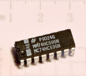
Figure 10-1. 74HC595 serial in, parallel out shift register
Note that the HCT family is designed for TTL input levels. I focus on the HC devices in this chapter because the device must interface to the CMOS-based Raspberry Pi.
74HC165 Pinout
Figure 10-2 provides a schematic pinout for the 74HC595 chip. Once again, different manufacturers use different labels for the various pins.
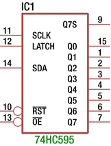
Figure 10-2. 74HC595 pinout
Table 10-1 documents the pins, the schematic labels, the NXP labels (not shown in Figure 10-2), and the pin functions for this chip.
Table 10-1. 74HC595 Pins and Functions
Pin | Schematic Label | NXP Label | Function |
|---|---|---|---|
11 | SCLK | SHCP | Shift clock |
14 | SDA | DS | Shift (in) data |
12 | LATCH | STCP | Latch (clock pulse) |
10 | RST | MR | (Master) reset |
13 | OE | OE | Output enable |
15 | Q0 | Q0 | Output Q0 (least significant bit) |
7 | Q7 | Q7 | Output Q7 (most significant bit) |
9 | Q7S | Q7S | Serial data output (for chaining) |
Function Table
Table 10-2 is an adaptation of the NXP-provided table, except that it uses the labels provided by the EAGLE software in Figure 10-2. In addition to the legend provided in Chapter 9’s Figure 9-3, there are two new symbols: NC, which means “No Change,” and Z, which means “high impedance” (essentially disconnected from the circuit).
Table 10-2. Function Table for 74HC595
Controls | Input | Output | ||||
|---|---|---|---|---|---|---|
SCLK | STCP | OE | MR | DS | Q7S | Qn |
X | X | L | L | L | L | NC |
X | ʿ | L | L | L | L | L |
X | X | H | L | L | L | Z |
ʿ | X | L | H | D | Q6S | NC |
X | ʿ | L | X | X | NC | QnS |
ʿ | ʿ | L | X | X | Q6S | Qns |
When the MR (reset) signal goes low (in the first line of the table), you can see that there are no changes on the outputs (Qn = NC), but it does clear the internal shift register. This is true whether the OE (output enable) signal is active or not (lines 2 and 3).
Line 3 shows you, however, that when the OE signal is inactive (high), the shift register outputs Q0 through Q7 (Qn) go into a high impedance (Z) state. In other words, these outputs become disconnected from the circuit that they are wired to.
Line 4 applies when MR is inactive (H), OE is active (L), and the signal SCLK (ʿ) goes from low to high. Here I used “D” to indicate a data bit is copied into the shift register bit Q0 (as ON Semiconductor does). The remaining shift registers’ cells are shifted to the next position. This results in the Q7 bit being replaced with the prior state of Q6. Note that the parallel latched outputs Q0 through Q7 remain unchanged (NC).
While OE remains active (L) in line 5, the rising signal STCP (ʿ) causes the shift register bits to appear externally at Q0 through Q7. This latching operation has no effect on the internal shift register contents, which is why output Q7S shows no change (NC).
The last line of the function table indicates that you can shift a data bit into the internal shift register and simultaneously latch that result so that it is externally visible. This can save a little bit of time in the output cycle.
Breadboard Experiment
Figure 10-3 illustrates the breadboard circuit for the 74HC595 chip. In this arrangement, you hardwire the OE pin to ground. This means that the outputs Q0 through Q7 will always be enabled. The clock pulses are wired to GPIO#5 as in the previous chapter. The LATCH signal is active when there is a low to high transition.
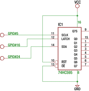
Figure 10-3. Breadboard circuit for 74HC595 output
You can take advantage of the /PL line as used in Chapter 9. Sharing that GPIO is possible because the input 74HC165 loads data while this line is low. The output 74HC595 will latch its outputs when the signal goes from low to high. You can, of course, use a different GPIO for this purpose if your application demands it. I’ll discuss GPIO sharing in more detail later.
Finally, you need GPIO #24 for passing data into the 74HC595 shift register from the Pi. You can use different GPIO assignments, but this is what the supplied source code will use for this experiment.
Lastly, this experiment ties the RST input to the +3.3V supply. This reset input is active low, so you tie it high so that it doesn’t become active for this experiment.
Unlike the 74HC165 input chip, you have no remaining inputs to wire to ground or the supply. CMOS outputs can be left without connections.
In the subdirectory hc595, you will find the Makefile and program hc595.cpp. Change to that directory and type make.
$ cd ./hc595$ makeg++ -c -std=c++11 -Wall -Wno-deprecated -Wno-narrowing -I. -I/usr/local/include/librpi2 -g -O0 hc595.cpp -o hc595.og++ hc595.o -o ./hc595 -L/home/pi/rpi2016/hc595/..//lib -lrpi2 -lrt -lmsudo chown root ./hc595sudo chmod u+s ./hc595
Once again, note that the program hc595 has been given setuid permission so that you won’t need to run it with sudo. Root permission is required to access the GPIO registers directly. Listing 10-1 shows the program area of interest.
Listing 10-1. Program hc595.cpp
008 #include "gpio.hpp"009010 static int hc595_latch = 16; // Outputs011 static int hc595_sclk = 5;012 static int hc595_sda = 24;013014 static unsigned usecs = 1;015 static GPIO gpio;016017 static void018 nap() {019 usleep(usecs);020 }021022 static void023 hc595_write(unsigned data) {024 unsigned b, temp = data;025026 gpio.write(hc595_sclk,0); // SCLK = low027 gpio.write(hc595_latch,0); // LATCH = low028 nap();029030 for ( int x=0; x<8; ++x ) {031 b = !!(temp & 0x80); // b = d7 (msb first)032 temp <<= 1;033 gpio.write(hc595_sda,b); // SDA = data bit034 nap(); // Wait035 gpio.write(hc595_sclk,1); // SCLK low -> high036 nap();037 gpio.write(hc595_sclk,0); // Complete clock pulse038 nap();039 }040 gpio.write(hc595_latch,1); // Latch data to outputs041 nap();042 printf("Wrote %02X to 74HC595\n",data);043 }
The main program (not shown) configures the GPIOs as outputs. If no command-line arguments are given, a call is made to hc595_write(0xD5) to transmit that bit pattern to the output chip. If other command-line parameters are provided, those values are written instead.
The hc595_write() routine starts by making sure that the SCK and LATCH signals are set to the low level (lines 026 and 027), followed by a delay. Line 024 has copied the data value into variable temp for use in the loop.
In the for loop of lines 030 to 039, this temp value is sampled at bit 7 and stored in variable b. The double !! operator just converts a nonzero result (in b) into the value 1 and otherwise to the value 0. Then line 032 shifts the variable temp one position to the left for the next loop iteration.
Line 033 writes the data bit value in b out to GPIO hc595_sda (GPIO #24). This establishes the high or low value to be shifted into the output register. Line 034 delays so that the signal transitions don’t happen too fast for the chip. Line 035 raises the clock signal (SCLK) from low to high. This will clock the data bit into the output chip. Line 037 returns the clock signal low again after a delay.
After all eight bits of data are shifted into the output chip, the LATCH signal is activated in line 040. Recall that it is the transition from low to high that makes the shift register chip’s output available on the chip output pins (Q0 through Q7). There is one more delay following this operation so that if the output routine gets called back to back, sufficient time will exist between signal changes.
Experiment Run
The schematic in Figure 10-3 did not have anything shown connected to the outputs Q0 through Q7. The experiment can be run without any connections if you have a DMM to measure the output levels with. Simply take a meter reading, and if the value is a high level, note a 1 bit.
If you want a visual indication, you can attach LEDs with a dropping resistor in series. Depending upon the manufacturer, the absolute maximum output of each pin is 25mA (Fairchild). The chip is further limited by its maximum power dissipation, when every output is driving full current. The Fairchild datasheet indicates 600mW as the absolute maximum power dissipation. If you limit each output to a maximum of 22mA, you just fit within that parameter.
Most LEDs will light with considerably less than this. Google LED voltage drop and you will find that many red LEDs will require about 1.8 volts. Taking this into account, you can compute the dropping resistor required.
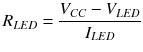
Assuming a modest current of 10mA for the LED and substituting allows you to compute the series dropping resistor.
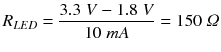
Figure 10-4 illustrates, in schematic form, the circuit necessary to attach to the output pins for Q0 through Q7. If you don’t mind moving the Dupont wires around, you can get by with just one LED.
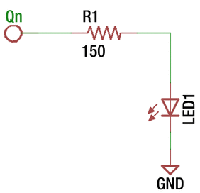
Figure 10-4. LED hookup with series dropping resistor
Running the program with no command-line arguments will output the hexadecimal value of D5.
$ ./hc595Wrote D5 to 74HC595
The hc595 program reports the value written to the 74HC595 chip. With this hex value (11010101 in binary), you should observe the following parallel data output:
Q7 is high.
Q6 is high.
Q5 is low.
Q4 is high.
Q3 is low.
Q2 is high.
Q1 is low.
Q0 is high.
Obviously, if you measure something else, then something is incorrect.
Input and Output
Let’s now look at combining the output 74HC595 with the input 74HC165 chips, using shared GPIO lines. Figure 10-5 illustrates the schematic circuit. IC1 is the 74HC595 that I’ve been discussing in this chapter, while IC2 is the added 74HC165 chip that was examined in Chapter 9.
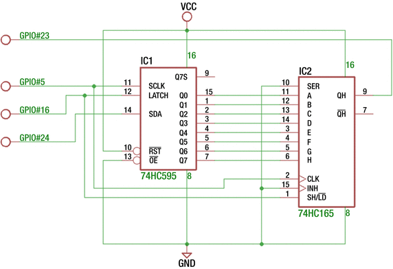
Figure 10-5. Combined output with input breadboard circuit
In this experiment, you’ve connected the outputs Q0 through Q7 to the inputs A through H of the 74HC165 chip. By doing this, your software should be able to output a value and then read it back as verification. The chip enable (INH) of IC2 has been wired to ground, since there is no need to select a chip. As before, the unused input SER of IC2 has also been tied to ground to eliminate any floating inputs.
The circuit shares GPIO #5 and GPIO #16 with both chips. GPIO #5 supplies the clock pulse, while GPIO #16 supplies the LD signal for IC2 and the LATCH symbol for IC1. The unshared GPIOs include #23 used for reading data, while GPIO #24 is used to supply data to IC1.
Listing 10-2 shows the interesting aspects of the code. Lines 010 to 013 allocate the GPIOs being used. Pin gpio_qh is the serial data in from the 74HC165, while gpio_sda is the serial data going out to the 74HC595. The gpio_latch and gpio_sclk lines are shared between the two chips.
Listing 10-2. Program hc165_595.cpp
010 static int gpio_qh = 23; // Input011 static int gpio_latch = 16; // Outputs012 static int gpio_sclk = 5;013 static int gpio_sda = 24;014015 static unsigned usecs = 1;016 static GPIO gpio;017018 static void019 nap() {020 usleep(usecs);021 }022023 static unsigned024 io(unsigned data) {025 unsigned b, ib, temp = data;026 unsigned idata = 0u;027028 gpio.write(gpio_sclk,0); // SCLK = low029 nap();030031 for ( int x=0; x<8; ++x ) {032 ib = gpio.read(gpio_qh); // Read 74HC165 QH output033 idata = (idata << 1) | ib; // Collect input bits034035 b = !!(temp & 0x80); // Set b to output data bit036 temp <<= 1;037038 gpio.write(gpio_sda,b); // write data bit039 nap(); // Wait040 gpio.write(gpio_sclk,1); // SCLK low -> high (shift data)041 nap();042 gpio.write(gpio_sclk,0); // Complete clock pulse043 nap();044 }045 gpio.write(gpio_latch,0); // Set new inputs046 nap();047 gpio.write(gpio_latch,1); // Latch data to outputs048 nap();049 printf("Read %02X, Wrote %02X\n",idata,data);050051 return idata;052 }
The function io() has been written to send and receive data. The data sent out is manipulated in temporary variable temp in lines 035 and 036. The data being read is accumulated in temporary variable idata in lines 032 and 033. At the conclusion, the values read and written are reported in line 049.
The main program invokes io() with values ranging from 0x00 through 0xFF and then the two additional values 0x00 and 0x01.
$ ./hc165_595Read 01, Wrote 00Read 02, Wrote 01Read 00, Wrote 02Read 01, Wrote 03Read 02, Wrote 04Read 03, Wrote 05Read 04, Wrote 06...snip...Read FB, Wrote FDRead FC, Wrote FERead FD, Wrote FFRead FE, Wrote 00Read FF, Wrote 01
The first value read (and reported) should be disregarded. It is reporting the current value in the shift register, which may be garbage the first time around. The second value also should be disregarded since this will represent the uninitialized value of the output register, as you will see.
Looking at the general pattern, you can see that the input values are two cycles behind what was last written. Here’s an example:
Read FC, Wrote FEHere you can observe that the read value was hexadecimal FC, while the currently written value is FE. The reason for this is subtle. Let’s break down the operations involved.
The LD signal of the 74HC165 goes low to capture its inputs, which is wired to the 74HC595 outputs Q0 through Q7.
When the LD signal returns high, the 74HC165 shift register holds 0xFC to send back to the Pi (this was the current 74HC595 output value).
However, in step 2, a low to high transition clocks in the new outputs for the 74HC595 outputs (which the 74HC165 chip has not yet seen).
The clock line shifts in eight more bits to the output IC1 chip, while the Pi reads the captured data in IC2.
Consequently, the Pi will read 0xFC, while just having written out 0xFE. The output value 0xFE will not be seen on the IC1 outputs until the next cycle’s step 2. These details can get confusing. Figure 10-6 illustrates my own breadboard experiment.
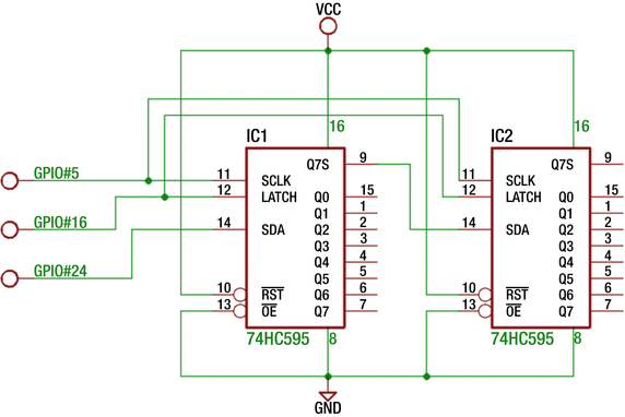
Figure 10-6. 74HC595 and 74HC165 breadboard experiment
Additional Outputs
Additional outputs can be had by adding another 74HC595 chip. Figure 10-7 shows the schematic for doing so. The SDA and LATCH signals are attached in parallel, and IC2’s data input comes from IC1’s output Q7S (pin 9).
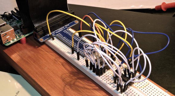
Figure 10-7. Two 74HC595 chips used for 16-bit output
Profit and Loss
The breadboard experiment in Figure 10-5 was a demonstration of eight outputs and eight inputs. These required four GPIO pins to manage it. This is a 400 percent improvement in GPIO ports. The cost, however, is the extra time required to shift in/out the data. The Figure 10-5 experiment illustrated that the total time was reduced by performing input and output simultaneously.
Summary
This chapter demonstrated how you can easily add GPIO outputs to your Pi for the cost of about $1. Even more outputs can be had with additional chips. Finally, you exercised both input and output chips simultaneously to gain 16 I/O pins using only four allocated GPIO ports.
Beyond the Pi’s GPIO ports used, the 74HC165 and 74HC595 chips required no software configuration, making them simple to use. The next chapter will introduce another way to add I/O pins to your Pi. But this will require software configuration.