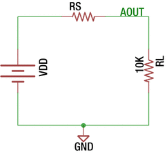
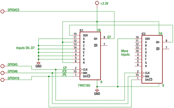
Economical text LCD displays are ideal for embedded Raspberry Pi applications where a full monitor is not required. The economical 16×2 LCD is popular with the Arduino crowd but can be used on the Raspberry Pi with a little extra work. Other similar LCD units can also be used if you need more lines or characters.
Many of these LCD modules use a parallel interface, which would require several GPIO lines. This chapter shows how to use a I2C interface module to overcome that disadvantage. These modules also use a 5V supply and require a 5V signal interface. This chapter presents a solution to this challenge.
LCD Module 1602A
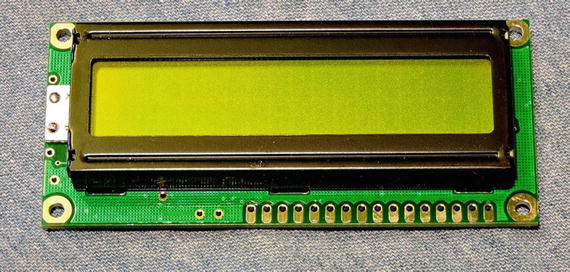
A search on eBay shows that the 1602A LCD module can be purchased for as little as $1.71 (the “Buy It Now” price). Figure 4-1 illustrates the topside of the unit, with its connections along the bottom.
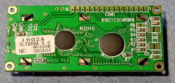
Figure 4-2 shows the bottom side of the module. The bottom side shows that connector CON1 has 16 connections. The number of connections is a nuisance from a wiring and interfacing standpoint, but there is a solution for that.
The logic and the LCD portions of this PCB require 5 volts, which makes this a little bit of a challenge for the Pi. But there is a solution for that too. The unit includes backlighting, so you must add the current for the logic plus the backlighting when planning your power requirements. The figures seem to vary depending upon the manufacturer, but one datasheet lists the current as 150mA for the logic plus another 100mA for the backlighting. So, this unit is likely to draw about 250mA total from your Pi’s 5V supply.
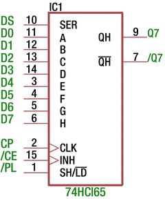
The 1602A module uses eight data lines and three control lines for data transfers. That would require 11 GPIO lines to be allocated from the Pi. However, it is possible to operate the module in 4-bit mode instead. This still requires seven GPIO lines, which is inconvenient.
To work around this problem, there is a nice I2C adapter module that can be economically purchased and used.
I2C Serial Interface
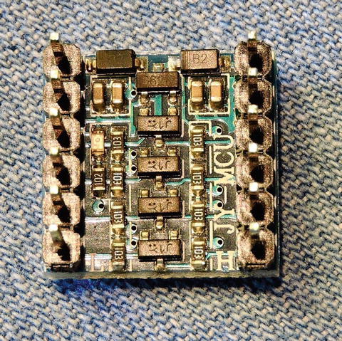
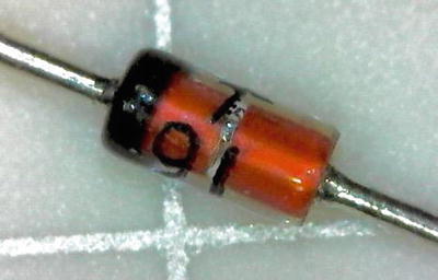
The module I purchased on eBay was titled “Black Arduino 1602LCD Compatible Serial Interface (IIC/I2C/TWI/SPI) Board Module.” The SPI in the title is bogus, since this is an I2C module. The module is based upon the PCF8574 chip, for which you can also obtain a datasheet.
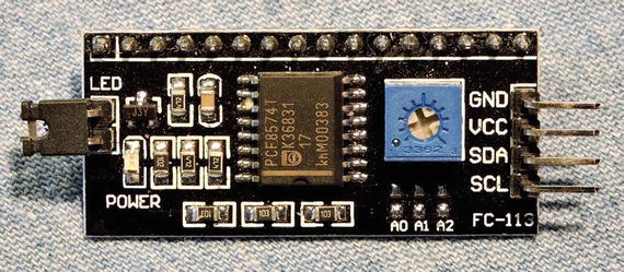
To find the module on eBay, search for 1602 serial module. I usually check the “Buy It Now” option so that there is no need to mess around with auctions and wait times. These modules can be purchased for as little as $1.10. Figure 4-3 illustrates the module that I purchased.
The module has three solderable jumpers marked A0, A1, and A2 (on the bottom right of Figure 4-3). Since CMOS inputs must not be left floating, there are pull-up resistors on the board. Based upon resistance readings taken, it appears that the three surface mount resistors marked “103” are the 10kΩ pull-up resistors to each of the address inputs. Soldering in a shorting jumper will change the address input to a logic 0.
Without any jumpers installed, this I2C PCB will respond to I2C address 27 hexadecimal (hex). With all jumpers installed, the I2C address changes to hex 20. If you should get a unit with the PCF8574A instead, the I2C address changes to 3F hex, with no jumpers or 38 with jumpers installed.
I have been unable to find a schematic for this exact PCB, but measuring between the VCC connection and the SDA or SCL connections confirms a resistance of 4–7kΩ (you can see resistors labeled “472” on the PCB). This evidence of a pull-up resistor is bad news for 3.3V operation because VCC on the PCB will be connected to 5 volts when used with the LCD module. The serial interface PCF8574 chip is able to operate from 3.3 volts, however, so before you connect it to the LCD module, let’s check the I2C module to see whether the unit is functional and usable by the Pi.
I2C Module Configuration
The PCF8574 peripheral is rather unique in that it does not require any formal configuration. The datasheet specifies that its ports are quasi-bidirectional. So, how does this work?
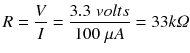
To set an output, you simply write a bit pattern to the outputs over the I2C bus. Pins written with a 1 bit turn off their pull-down transistor and cause the pull-up current source to bring the output pin high. This pull-up current source is weak, supporting only 100μA. The NXP documentation indicates, however, that there is an accelerated strong pull-up that is active during the high time of the I2C acknowledge clock cycle. This briefly helps the output turn sharply high at the right time but requires only 100μA to maintain that state after. This works fine for interfacing to CMOS input signals. But because of the weak high-side drive, the ports cannot source current into LEDs.
Output ports that are written with a 0 bit cause their pull-down transistor to activate to conduct port current to ground level. This driven output can sink up to 25mA of current, though the chip total must not exceed 80mA. This makes the port capable of driving LEDs when the ports are used to sink LED current.
To be able to read an input, there is a cheat step required: the port must first be written with a 1 bit so that its weak pull-up current source can allow the port to rise high. Then the component driving the input can pull the voltage down to ground level when transmitting a 0 bit to the input. When a 1 bit is transmitted to the port, the signal is simply brought high again with some assistance from the weak pull-up current source.
If the input port was left in the output 0 bit state, the port’s output driver transistor would keep that port grounded. To indicate a 1 bit, the component driving this input would have to overcome this with a struggle. This could result in high currents and potential damage.
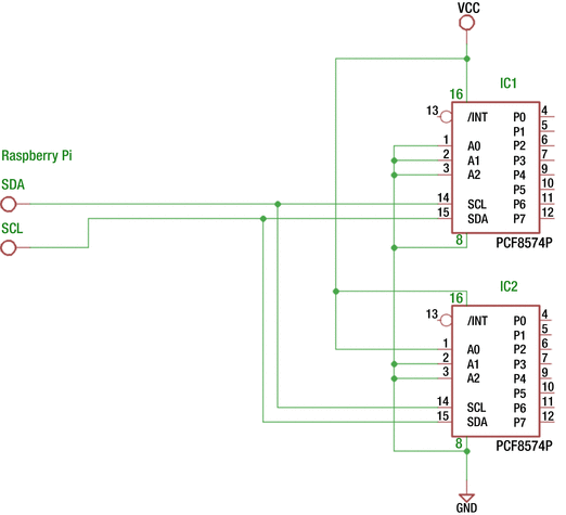
I2C Module Output
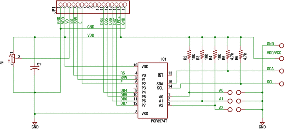
Figure 4-4 is a generic schematic of the different I2C modules available. For this experiment, don’t attach the LCD display yet, since the display module will not function on 3.3 volts. But the wiring of the unit is important to note because you need to know where the port pins appear on the edge of the PCB.
From Figure 4-4 you can see that four of the outputs go to pins 11 to 14 of the 16-pin header strip. These will be used to send four bits at a time to the LCD module. These are port bits 4 through 7, respectively. Three of the four remaining bits go to the LCD interface pins 4, 5, and 6 to control the information handshaking. These are pins 0 through 2, respectively, with port pin 3 left unconnected (on some LCD modules, pin 3 switches backlighting on or off).
Table 4-1 summarizes the port pins and the corresponding LCD pins for your convenience.
Table 4-1. Port Locations on the 16×1 LCD Header Strip
P0 | 4 | LCD RS |
P1 | 5 | LCD R/W |
P2 | 6 | LCD E |
P3 | Internal | Backlighting switch, when supported by I2C module |
P4 | 11 | LCD DB4 |
P5 | 12 | LCD DB5 |
P6 | 13 | LCD DB6 |
P7 | 14 | LCD DB7 |
Let’s first verify that the I2C bus is available, as shown here:
$ i2cdetect -l
i2c-1 i2c        3f804000.i2c                     I2C adapter
If i2cdetect is not installed, then install it now, as shown here:
$ sudo apt-get install i2c-tools
Now that you have confirmed that the I2c-1 bus is available, attach the serial module (without the LCD connected). Connect the V
CC
to the Pi’s 3.3V supply and GND to the Pi’s ground. Finally, connect SDA and SCL to the Pi’s SDA and SCL connections, respectively (the T-Cobbler silk screen should identify these plainly).
With this wired up, start your Pi and perform the following scan of I2C bus 1, as shown here:
$ i2cdetect -y 1
     0  1  2  3  4  5  6  7  8  9  a  b  c  d  e  f
00:          -- -- -- -- -- -- -- -- -- -- -- -- --
10: -- -- -- -- -- -- -- -- -- -- -- -- -- -- -- --
20: -- -- -- -- -- -- -- 27 -- -- -- -- -- -- -- --
30: -- -- -- -- -- -- -- -- -- -- -- -- -- -- -- --
40: -- -- -- -- -- -- -- -- -- -- -- -- -- -- -- --
50: -- -- -- -- -- -- -- -- -- -- -- -- -- -- -- --
60: -- -- -- -- -- -- -- -- -- -- -- -- -- -- -- --
70: -- -- -- -- -- -- -- --
The session output confirms that the I2C device is seen as address 27 (hex). This is a good sign that the device is working. If you have a different model of the PCB, you may find the unit at a different address, perhaps 3F. Substitute your address in the tests that follow.
Change to the subdirectory pcf8574 in the supplied source code. Perform a make command (if not already performed), which should leave you with an executable named i2cio. The command takes optional arguments, which are explained with the use of the help (-h) option.
$ ./i2cio -h
./i2cio [-a address] [-i pins] [-h] [out_value1...]
where:
       -a address  Specify I2C address
       -i 0xHex    Specify input port pins (0=none=default)
       -h          Help
If your unit was found at a different address than the default hexadecimal address of 27, then you will need to supply that in the commands afterward with the option -a.
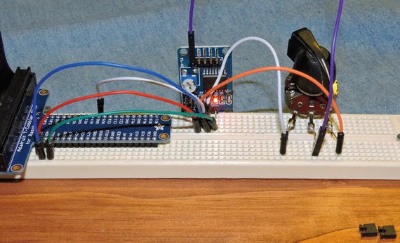
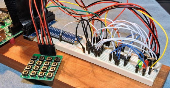
I recommend doing this experiment with Dupont wires only since it is easy to cause a short circuit and ruin something. Either place the PCB module on the breadboard and connect to it through the breadboard or locate some male/female Dupont wires to safely attach your connections.
Connect the negative lead of your voltmeter/DMM to the ground of the Pi. Using the plus lead of the DMM, measure the voltage present at pin 14 of the 16×1 header strip. You should measure either 3.3 volts or 0 volts. Now run the following command (substituting for the I2C address if necessary). Do not omit 0x where it appears, as this specifies that the number is in hexadecimal notation.
$ ./i2cio -a0x27 0x80
I2C Wrote: 0x80
This command writes the hex value 80 to the I2C port at address 27. After this runs, you should measure approximately 3.3 volts at pin 14. If you don’t get that, then check that you have the correct pin. My PCB unit marks pin 16 with a square, suggesting it is pin 1, but this is actually pin 16.
To confirm the port’s operation, let’s now write a 0 out.
$ ./i2cio -a0x27 0
I2C Wrote: 0x00
After the message I2C Wrote: 0x00, you should immediately see the voltage go to 0 on pin 14. This confirms the following:
That the unit is operating and responding to the I2C address you specified
That port bit 7 corresponds to connection 14 on the header strip
That you know which end of the header strip is pin 1
This last item is important since it is easy to get this wrong. Cheap clones of the original board are being made all the time, and important matters like this are often incorrect or mislabeled.
Now check bit 4, using the value 0x10, followed by setting it to 0. Did pin 11 on the PCB module obey? Finally, using the value 0x01, does the RS signal (header pin 4) measure the correct changes?
I2C Module Input
Having succeeded in performing I2C output to the module, it is now time to try input. Connect a Dupont wire to header pin 14 (DB7) and the other end to your breadboard. Just leave it unconnected for the moment and perform this test:
$ ./i2cio -a0x27 -i0x80
I2C Read: 0x80 (Inputs: 80)
By adding the option -i0x80, you have made bit 7 an input. This was done by first setting the output bit to a 1 so that inputs could be performed on it. The command then performs a read and reports what it read. In this case, only the high bit is significant, and since 0x80 indicates a high value, you know the input bit was a 1.
If you don’t want to see the other bits, you can force the others to 0 by doing an output first and then repeating the following:
$ ./i2cio -a0x27 0
I2C Wrote: 0x00
$ ./i2cio -a0x27 -i0x80
I2C Read: 0x80 (Inputs: 80)
After setting all output bits to 0, only the input should ever show up as a 1 bit.
Before running the command again, connect your input Dupont wire to ground. When you perform the read test this time, the reading should change, as shown here:
$ ./i2cio -a0x27 -i0x80
I2C Read: 0x00 (Inputs: 80)
Again, only the high bit (7) is significant since that is the only input you’re polling. You can see from the value reported that the grounding of that pin caused the command to read 0. Unground the Dupont wire and repeat. Did the read value change back to 0x80?
PCF8574P Chip
From the preceding experiments you can see that this module can be used as a cheap and nearly configuration-free I2C GPIO extender. The main issue is that the PCB is designed to work with the 1602A LCD. This might mean that only seven of the eight GPIOs are brought out to the header strip (the blanking bit may be supported, however, to make eight).
The PCF8574P chip is available in the plastic DIP form from various sources including eBay, for as little as $0.66. Since this chip will operate at 3.3 volts, it is a good trick to keep in your back pocket when adding GPIOs to the Raspberry Pi. With no complicated software configuration required, it is quite easy to use. Just keep in mind that when driving a current load (like an LED), always arrange the port to sink the current.
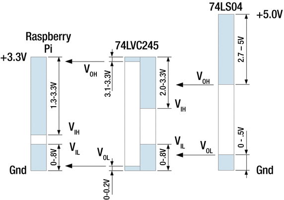
3 Volts to 5 Volts
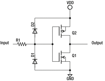
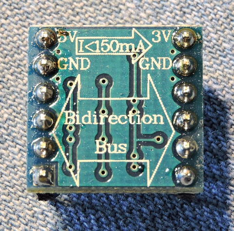
The LCD module must operate at 5 volts. So, now you must cross that digital divide from the 3.3V realm to the 5V TTL world. Note that Chapter 2’s techniques do not apply to the I2C bus, so you must find another way to do this. Figure 4-5 shows a tiny little level converter with the header strips installed. On eBay, you can purchase these for a “Buy It Now” price of $0.99.
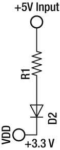
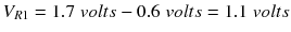
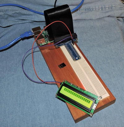
Figure 4-6 shows the bottom-side silk screen. There is a 3V output derived from the 5V input, shown on the top right of the figure. But I recommend you use that as a last resort. Use the Pi’s 3.3V power instead because I have found that this connection can be higher than it should be. If you do use it, the silk screen indicates that it is limited to 150mA.
There are four remaining pins on the left and right sides. The idea is that on one side you have your 5V signals and on the right are the 3.3V signals. This device is bidirectional, using MOSFET transistors to do the level conversions. For these purposes, you need the I2C SDA and SCL lines converted.
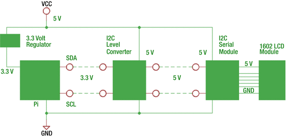
To keep the various systems in perspective, Figure 4-7 illustrates the signal realms involved, including the Raspberry Pi on the left, the level converter at the center, and the 5V I2C serial module for the LCD on the right.
The dashed lines of Figure 4-7 illustrate the I2C signals as they progress from the Pi to the I2C serial module at the right. Except for the fact that this level conversion adds another module to the mix, the circuit remains otherwise simple. The two I2C signals SDA and SCL are all that are required to communicate with the LCD module.
Attaching the I2C Serial Module
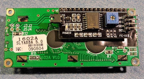
Take a good look at Figures 4-2 and 4-3. Note particularly where pin 1 of CON1 is shown in Figure 4-2. This pin is near the mounting hole in the upper right of the photo. This is where pin 1 of the I2C serial adapter needs to go.
On my serial adapter, the silk-screen square is shown at the top left. This is incorrect! Using a DMM, I was able to confirm that V0, which is pin 3, is actually the third pin from the top right of Figure 4-3. I seem to have a clone of the original design where they botched the silk screening. The PCB square should have been at the top right instead. I mention this to save you a lot of agony. Once the PCB is soldered to the LCD module, it is difficult to separate them. Take your time getting the orientation correct before you plug in that soldering iron.
Figure 4-8 shows the I2C module installed on the LCD module. The power and the two I2C connectors should be located at the upper right. I put a piece of electrical tape underneath the I2C module before soldering it in place. This will keep bare connections from bumping into connections on the LCD module.
I like to test things as I go since this saves a lot of troubleshooting effort when things go wrong and provides a confidence boost when things are going right. The best way to do this is to yank the microSD card out of the Pi so that it doesn’t boot. That way, if something goes wrong, you can yank the power without having to worry about corrupting the microSD card. It also saves you from having to do a formal shutdown when you’re done testing.
As part of this test, adjust the potentiometer so that you start to see the character cells in the display. You’ll likely readjust again, once text is shown on the display later. My LCD module initialized such that one line of cells was showing. Yours may show a different pattern. Even if you get no pattern at all, don’t panic about it until you try sending data to it under software control.
If you want to take a current reading, this is a good time to do it. While my LCD was operating under test in Figure 4-9, I measured about 87mA of current. On the I2C module, there is a jumper at one end. Removing it turns off the backlighting for the module by disconnecting the power for it. Once I did this, the current dropped to about 6mA. If you have a battery-operated system, you could save power this way.
The next step is to hook up the I2C level converter. Wire the Pi’s +5 volt to the level converter’s 5V input and its ground to ground. Also connect the serial module SDA and SCL lines to the 5V side of the level converter, but save the 3.3V SDA and SCL for later. Leave those unconnected. Using your voltmeter/DMM, measure the 3.3V SDA and SCL pins on the level converter when powered. You should get a reading near 3.3 volts. If you read something else, you need to investigate. If the voltage reads higher than +3.6 volts, then don’t go any further since hookup could damage your Pi’s GPIO ports. Once you have good readings, you are clear to connect the Pi’s SDA and SCL ports to the level converter’s 3.3V side.
Displaying Data
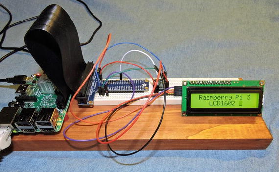
Once everything is wired, you are ready to display some data on the LCD. Figure 4-10 illustrates the LCD connected to the Pi with some text displayed. In the subdirectory pcf8574, there is a program named lcd.cpp that should have been built as executable lcd. If the executable does not yet exist, type the make command now to build it.
Invoke the command simply as follows:
$ ./lcd
If all went well, you should see the same text as displayed in Figure 4-10. The trickiest part is getting the LCD module to initialize, partly because you must operate in the LCD controller’s 4-bit mode.
The initialization procedure for 4-bit operation is a little strange. The HD44780 controller chip used by the display always powers on in the 8-bit communication mode. Because you are going through the PCF8574 and using four of those bits for controlling the signal handshaking, only the upper four data bits are being seen by the controller when you write to it.
Inside the class method LCD1602::initialize(), the following is done to coax the LCD controller into using 4-bit mode. The reusable source files are lcd1602.cpp and lcd1602.hpp, should you want to use it in your own code.
165     usleep(20000);          // 20 ms
166     lcd_write4(0x30);       // 8-bit mode initialize
167     usleep(10000);          // 10 ms
168     lcd_write4(0x30);
169     usleep(1000);           // 1 ms
170     lcd_write4(0x30);
171     usleep(1000);           // 1 ms
172     lcd_write4(0x20);       // 4-bit mode initialize
173     usleep(1000);           // 1 ms
Line 165 just begins with a delay in case there was recent activity with the display. Line 166 calls upon internal class method lcd_write4() to write out the 8-bit command 3X, where X represents garbage (likely seen as 3F by the controller). You do this three times and then finally set the mode you really want in line 172. This sets the controller into 4-bit mode.
After this point, all 8 bits of a command or data byte are sent as two back-to-back 4-bit writes (using the method lcd_cmd() or lcd_data()). Each write is preceded by a busy check, by reading from the controller. When it reads that bit 7 is no longer a 1, it then knows that it is safe to write into the controller again. This is performed in method lcd_ready() for the curious.
Reading from the LCD1602
Except for the initialization sequence, the code driving the LCD does not use delays. This has the benefit of increasing the data rate to almost as fast as the device will accept it. The initialization sequence, however, requires the use of delays since the controller does not provide any busy status during that time. Once initialized, there is a busy status flag that can be read.
Reading the status from the LCD controller is tricky when conversing through the PCF8574 in 4-bit nibbles. Recall that to read an input from the PCF8574, you must first write a 1 bit to the pin first. Since the status is available immediately after an LCD command write, you have to be careful in how you perform this.
Steps 1 through 4 are all that are required to send an 8-bit command to the LCD controller through the PCF8574 chip (Table 4-2). Some LCD commands, however, such as “clear screen,” require extra time to complete. If you sent another command byte during this busy period, the command would be ignored. You could use a programmed delay, but different LCD commands take different amounts of time. It is best to have the LCD controller tell you when it is no longer busy.
Table 4-2. Steps Used to Write One 8-Bit Command and Read the BF Status Flag
1 | bit 7 | bit 6 | bit 5 | bit 4 | bl | 1 | 0 | 0 | Write | Enable write of high command nibble. |
2 | bit 7 | bit 6 | bit 5 | bit 4 | bl | 0 | 0 | 0 | Write | Clock in the high command nibble. |
3 | bit 3 | bit 2 | bit 1 | bit 0 | bl | 1 | 0 | 0 | Write | Enable write of low command nibble. |
4 | bit 3 | bit 2 | bit 1 | bit 0 | bl | 0 | 0 | 0 | Write | Clock in the low command nibble. |
5 | 1 | 1 | 1 | 1 | bl | 0 | 1 | 0 | Write | Prepare to read (RW=1) and set bits 7, 6, 5, and 4 to 1 so that you can read from those ports. |
6 | 1 | 1 | 1 | 1 | bl | 1 | 1 | 0 | Write | Prepare LCD to present status. |
7 | BF | AC6 | AC5 | AC4 | X | X | X | X | Read | Read upper status nibble. |
8 | 1 | 1 | 1 | 1 | bl | 0 | 1 | 0 | Write | Complete the upper nibble read. |
9 | 1 | 1 | 1 | 1 | bl | 1 | 1 | 0 | Write | Prepare LCD to present lower nibble. |
10 | AC3 | AC2 | AC1 | AC0 | X | X | X | X | Read | Read lower status nibble. |
11 | 1 | 1 | 1 | 1 | bl | 0 | 1 | 0 | Write | End read cycle. |
12 | Repeat, starting at step 6 when BF=1, until BF=0 (ready) | | | | | | | | | |
Before you look at the read cycle, I’ll explain what happened during the write steps. Step 1 sets the BL bit to 1 if you want to keep the backlighting enabled. This bit is ignored if the I2C adapter doesn’t support this feature. The RS=0 bit indicates that a command byte is being sent. Bit RW=0 indicates to the LCD controller that a write operation is being performed. Finally, E=1 prepares the LCD controller to receive 4 bits of data on bits 7, 6, 5, and 4. In 4-bit handshaking, the remaining bits of the data bus are ignored. Keep in mind that these bits are being written over the I2C bus into the PCF8574 chip and appearing at the chip’s own GPIO pins, which are interfaced to the LCD module (review Figure 4-7).
No data is captured in the LCD controller yet, until step 2. In this step, the signal E=0 is established (by another I2C write operation). The transition from E=1 to E=0 clocks the data into the controller (the high nibble). Steps 3 and 4 repeat steps 1 and 2, except that the low-order nibble is transmitted. Once step 4 has completed, the LCD controller has received eight bits of command data and begins to carry it out.
To know when it is safe to send another command (or data), you must ask the LCD controller for the BF (busy flag) status bit. To prepare for a read from the PCF8574, you must first write 1 bits to bits 7, 6, 5, and 4, where you expect data. Additionally, RW=1 is established to warn the LCD controller that you will be performing a read operation. This is what step 5 is all about.
Nothing happens on the LCD controller until it sees the E signal change from 0 to 1 in step 6. At this transition, the controller puts the status byte out to its data lines. At this point, the controller is driving bits 7, 6, 5, and 4 of the PCF8574 pins. Step 7 tells the PCF8574 chip to take a reading and send it back to the Pi on the I2C bus. Table 4-2 has an X marked in the remaining positions as “don’t care.” You are only receiving data transferred in the upper nibble of this byte read.
Steps 8 through 10 repeat steps 5 through 7, except this time the lower nibble of data is transferred. Step 11 ends the read cycle and informs the LCD controller you are done.
Now the BF flag is examined. When BF=1, the LCD controller is still busy carrying out the last command. The Pi program then repeats again starting from step 6. This repeats until the controller finally returns BF=0, indicating “ready.”
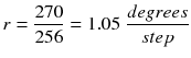
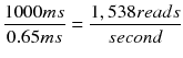
How long does all of this take? With I2C operating at 100kHz, each byte takes approximately the following amount of time:
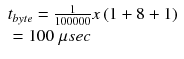
There is a start bit, eight data bits, and one stop bit for each I2C byte written to the PCF8574. So, assuming you don’t receive BF=1, the write followed by a status read should take approximately this long:

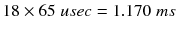
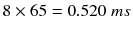
This means you can issue approximately 909 LCD commands per second, ignoring busy wait times. From my own testing, I found that most commands do not incur any busy time because of the time involved in the I2C traffic. The only instance I encountered where BF=1 was in clearing the screen. Given that it takes seven I2C cycles to read the LCD status, this results in a delay of 100 × 7 = 700μsec of time. Most LCD commands complete in much shorter times (consult the HD44780 controller datasheet for actual times).
Given these facts, it is tempting to program delays instead. But it is best to consult the BF status flag because if the LCD controller should miss a command or data byte, you would have no knowledge of it in your program. The display would continue in a messed-up state until it was reset by your code.
Class LCD1602
I2C programming is covered in Chapter 11, so I won’t repeat that here. However, the source code includes the following two files in the pcf8574 subdirectory:
Include the class definition in your program with the following:
#include "lcd1602.hpp"
Then you can make use of the LCD1602 class to interact with your display. To instantiate the class, you code it with the optional I2C address and bus number, as shown here:
LCD1602 lcd(0x27,1); // I2C address and bus number
After this, you need to initialize it only once, as shown here:
if ( !lcd.initialize() ) {
    fprintf(stderr,
        "%s: Initializing LCD1602 at I2C bus %s, address 0x%02X\n",
        strerror(errno),
        lcd.get_busdev(),
        lcd.get_address());
    exit(1);
}
From that point on, in your own code you can invoke the public functions such as lcd.clear() and lcd.putstr(). The following is a summary of the public members of the LCD1602 class:
class LCD1602 {
        ...
public: LCD1602(unsigned i2c_addr=0x27,unsigned bus=1);
        ∼LCD1602();

        const char *get_busdev() const  { return busdev.c_str(); };
        unsigned get_bus() const        { return i2c_bus; }
        unsigned get_address() const    { return i2c_addr; }

        bool initialize();              // Initialize the LCD
        bool lcd_ready();

        bool lcd_cmd(uint8_t byte)      { return lcd_write(byte,true); }
        bool lcd_data(uint8_t byte)     { return lcd_write(byte,false); }

        bool clear();
        bool home();
        bool moveto(unsigned y,unsigned x);

        bool putstr(const char *str);

        bool set_display(bool on=true);
        bool set_blink(bool on=true);
        bool set_backlight(bool on=true);
        bool set_cursor(bool on=true);

        bool get_display() const        { return display; };
        bool get_blink() const          { return blink; };
        bool get_backlight() const      { return backlight; };
        bool get_cursor() const         { return cursor; };
};
If you want to learn more about the features of the LCD module, locate the HD44780 controller’s datasheet in PDF form. That document will describe all the commands and features supported by the controller.
I2C Baud Rate
Throughout this book, the default system I2C baud rate is used. You can discover what that rate is with the following command:
$ dmesg | grep -i i2c
[5.102698] bcm2708_i2c 3f804000.i2c: \
           BSC1 Controller at 0x3f804000 (irq 83) (baudrate 100000)
From this you can see that the I2C driver initialized with the baud rate of 100kHz (100,000). This is not particularly fast but is considered reliable. The I2C level shifter used in this chapter also limits the reliability of the connection and probably shouldn’t be pushed much higher. Despite the I2C bus operating at 100kHz and using 4-bit I/O transfers, you’ll still find that the display is responsive. A simple LCD command structure and the fact that the display holds only 32 characters means that the I/O system is not unduly taxed.
Profit and Loss
In this chapter’s project, you used a level translator and a PCF8574 I2C extender on a PCB to communicate with the 1602 LCD module. Let’s review some of the pros and cons of doing this.
Here are the pros:
Only two lines are needed for communicating to the LCD from the Pi.
I2C allows a few meters of distance between the Pi and LCD.
Only two GPIOs are required from the Pi side.
The PCF8574 I2C module might provide backlighting control.
The 1602 LCD, PCF8574 PCB, and level translator are all inexpensive.
Here are the cons:
The method requires commanding the LCD module in 4-bit mode.
The PCF8574 I2C module is slower driving the LCD.
The LCD module is 5 volts, requiring a level translator.
Configuration of the LCD is limited.
Certainly there is some complexity involved with the added components, but the overall cost is low. Because communication occurs over the I2C bus, the LCD can be a few meters away from the Pi itself.
The one negative I saw was that there seems to be no way to configure the LCD module for other modes of operation in 4-bit data transfer mode. The command 0x20 is used to put the LCD controller into 4-bit mode (note that this is sent in 8-bit mode). This works because the 2 in 20 is in the upper nibble that the controller can see. But the lower nibble of that “function set” command consists of the N and F bits that allow two-line (N=1) or one-line (N=0) displays and a 5 × 10 dots (F=1) or 5 × 10 dots (F=0) font.
In my own experiments, the configuration always went to N=1, leaving F to be ignored (the LCD won’t do two-line displays with the larger font). I suspect that this is the result of the low nibble signals being pulled high by the LCD module (these are unconnected). This results in the controller seeing N=1. This is not too much of a hardship given that most people will want the two-line display more than the larger font in one line.
Summary
This chapter covered a lot of ground, partly because of the challenges faced by using a 5V I2C part. Additionally, the PCF8574 GPIO extender was applied to reduce the number of lines required to drive the display. By using the I2C communication bus, it becomes possible for your LCD display to be a few meters away from the Pi. The best part is that the LCD display is cheap, is readily available, and requires only power and two lines of communication.